Wafer processing method and wafer obtained by the wafer processing method

A processing method and wafer technology, applied in electrical components, semiconductor/solid-state device manufacturing, circuits, etc., can solve the problems of wafer glue residue, inability to properly maintain the wafer itself, etc., to prevent glue residue and achieve good results. Effect

Inactive Publication Date: 2014-05-21
NITTO DENKO CORP
View PDF7 Cites 0 Cited by
  • Summary
  • Abstract
  • Description
  • Claims
  • Application Information

AI Technical Summary

Problems solved by technology

In this cleaning process, the adhesive layer of the adhesive sheet dissolves or swells due to the solvent used for cleaning, and sometimes the wafer itself cannot be properly hel

Method used


Image

  • Wafer processing method and wafer obtained by the wafer processing method

Examples


Example Embodiment

[0069] [Manufacturing Example 1] Preparation of adhesive composition

[0070] To 100 parts of resin component (manufactured by TORAY COATEX CO., LTD., trade name: Rheocoat R-1020), 3 parts of isocyanate-based crosslinking agent (manufactured by Nippon Polyurethane Industry Co., Ltd., trade name: CORONATE L) as a crosslinking agent , 3 parts of photopolymerization initiator (manufactured by BASF Corporation, trade name: IRGACURE651) and 70 parts of UV curable oligomer (manufactured by Nippon Kayaku Co., Ltd., trade name: KAYARAD DPHA) were stirred to obtain an adhesive composition.

Example Embodiment

[0071] [Production example 2] Production of adhesive sheet for wafer processing

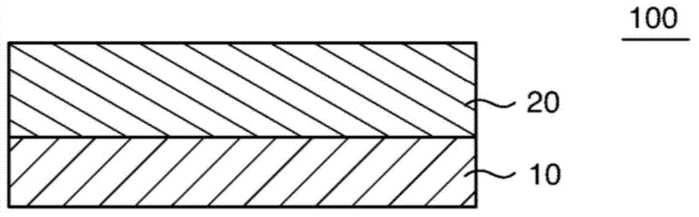
[0072] The adhesive composition obtained in Production Example 1 was applied to the release-treated surface of a release-treated film with a thickness of 38 μm so that the thickness after drying was 20 μm, and dried at 120°C for 2 minutes using a dryer , Form an adhesive layer. This adhesive layer and the base material (polyethylene film) were bonded together to obtain an adhesive sheet for semiconductor wafer processing.

Example Embodiment

[0073] [Example 1]

[0074] The PET film was peeled off from the adhesive sheet for wafer processing obtained in Manufacturing Example 2, and the wafer and the ring for wafer processing were bonded together using a bonding device. Next, ultraviolet rays were irradiated from the adhesive layer side of the wafer processing adhesive sheet (the side where the wafer and the wafer processing ring were laminated) under the following conditions so that the adhesive layer did not contact the wafer and wafer The part in contact with the ring for wafer processing is cross-linked. Next, methanol as a solvent is sprayed from the wafer and wafer processing ring side of the laminated body of the wafer processing adhesive sheet and the wafer and the wafer processing ring to clean the wafer. Then, ultraviolet rays were irradiated from the substrate side under the following conditions to peel off the adhesive sheet for wafer processing from the wafer.

[0075]

[0076] Device: manufactured by Nitt...


PUM


Abstract

The present invention provides a wafer processing method and a wafer obtained by the wafer processing method. The wafer processing method comprises a solvent cleaning step before a random appropriate processing step is performed, wherein a wafer can be properly kept and residual adhesive after stripping of a binding sheet is prevented in the processing step. The wafer processing method of the invention comprises the steps of: a binding sheet binding step for binding the wafer on the binding strip which is provided with a substrate and an adhesive layer with radiating-ray curable adhesive; a radiating ray irradiating step of irradiating radiating ray on the adhesive layer of the binding sheet for processing the wafer; the cleaning step of cleaning the wafer by the solvent; and a processing step of processing the wafer. In the wafer processing method of the invention, the radiating ray irradiating step is performed before the cleaning step.

Description

technical field [0001] The present invention relates to a wafer processing method and a wafer obtained by the wafer processing method. Background technique [0002] In the wafer processing step, an adhesive sheet is used to properly hold the wafer during processing. In the wafer processing process, in order to remove foreign matter adhering to the wafer and / or peel off the protective film of the wafer, the wafer attached to the adhesive sheet may be cleaned before performing any appropriate processing steps. process (for example, Patent Document 1). In this cleaning step, the adhesive layer of the adhesive sheet dissolves or swells due to the solvent used for cleaning, and sometimes the wafer itself and the wafer processing ring used for wafer processing cannot be properly held. In addition, when the adhesive sheet is peeled off after the processing process, adhesive residue may be generated on the wafer. In order to solve such a problem, for example, a PSA sheet includin...

Claims


Application Information

Patent Timeline
IPC IPC(8): H01L21/02H01L21/683
CPCH01L21/02005H01L21/02057H01L21/6836H01L21/52
Inventor 杉村敏正田中俊平高桥智一秋月伸也
Owner NITTO DENKO CORP
Why Eureka
Try Eureka