Chip appearance detection method and system

A technology of appearance inspection and chip, which is applied in the direction of measuring devices, optical testing flaws/defects, instruments, etc., can solve the problems of slow detection speed and low detection efficiency, and achieve the effect of automatic identification and avoiding slow detection speed

Inactive Publication Date: 2011-03-30
BYD CO LTD
View PDF0 Cites 50 Cited by
  • Summary
  • Abstract
  • Description
  • Claims
  • Application Information

AI Technical Summary

Problems solved by technology

[0005] The purpose of the embodiment of the present invention is to provide a chip appearance detection method, aiming to solve the problem that in the prior art, the manufacturer adopts the

Method used


Image

  • Chip appearance detection method and system
  • Chip appearance detection method and system
  • Chip appearance detection method and system

Examples


Embodiment Construction

[0019] In order to make the object, technical solution and advantages of the present invention more clear, the present invention will be further described in detail below in conjunction with the accompanying drawings and embodiments. It should be understood that the specific embodiments described here are only used to explain the present invention, not to limit the present invention.

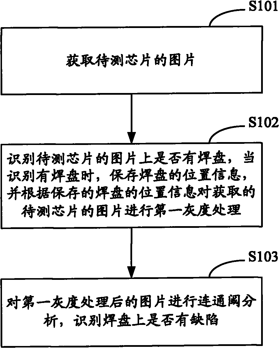
[0020] In the embodiment of the present invention, when it is recognized that there is a pad on the picture of the chip to be tested according to the shape feature of the pad, the pad shape feature information is saved, and after the grayscale processing is performed on the acquired image, the connected domain analysis is used to extract the Defects in grayscaled images.

[0021] figure 1 The flow chart of the chip appearance detection method provided by the embodiment of the present invention is shown.

[0022] In step S101, a picture of the chip to be tested is acquired.

[0023] Specifical...


PUM


Abstract

The invention provides chip appearance detection method and system, which is applicable to the technical field of chip appearance detection, wherein the method comprises the following steps of: obtaining a picture of a chip to be tested; identifying whether a welding disc exists on the picture of the chip to be tested or not; storing the position information of the welding disc when the existenceof the welding disc is identified, and carrying out primary gray processing on the obtained picture of the chip to be tested according to the stored position information of the welding disc; carryingout communicated region analysis on the picture of the chip to be tested after the first gray processing; and identifying whether defects exist on the welding disc or not. The automatic identification of appearance defect of the welding disc on the chip can be realized, and the problems of low detection speed and low detection efficiency caused by welding disc defect of the manual eye detection mode can be avoided. In addition, after the step of obtaining the picture of the chip to be tested and before identifying whether the welding disc exists on the picture of the chip to be tested or not according to the shape characteristic of the welding disc, whether the dimension of the chip to be tested is qualified or not can be judged through extracting the dimension data of the chip to be tested and comparing the obtained data to the stored chip dimension data.

Description

technical field [0001] The invention belongs to the technical field of chip appearance inspection, and in particular relates to a chip appearance inspection method and system. Background technique [0002] At present, in the production process of silicon microphones widely used in high-tech electronic products such as notebook computers and mobile phones, strict inspections must be carried out on each step in the production process to eliminate unqualified products to ensure the quality of the silicon microphones leaving the factory. quality. [0003] Since the appearance of the silicon microphone chip directly affects the performance of the silicon microphone, especially for the pad on the front of the silicon microphone, when dust or scratches enter the pad, it will directly affect the pronunciation performance of the silicon microphone. The appearance of the pads on the chip is inspected before the microphone leaves the factory. [0004] In the prior art, the manufactur...

Claims


Application Information

Patent Timeline
IPC IPC(8): G01B11/03G01B11/24G01B11/02G01B11/28G01N21/88
Inventor 刘杰刘瑛王艳
Owner BYD CO LTD
Why Eureka
Try Eureka