Optical proximity correction method

An optical proximity correction and optical technology, applied in the field of lithography, can solve problems such as long time-consuming and affecting production efficiency, and achieve the effect of improving production efficiency and shortening time

Active Publication Date: 2011-03-30
STATE GRID CORP OF CHINA +2
View PDF0 Cites 34 Cited by
  • Summary
  • Abstract
  • Description
  • Claims
  • Application Information

AI Technical Summary

Problems solved by technology

[0006] The problem solved by the invention is that conventional optical

Method used


Image

  • Optical proximity correction method
  • Optical proximity correction method
  • Optical proximity correction method

Examples


Embodiment Construction

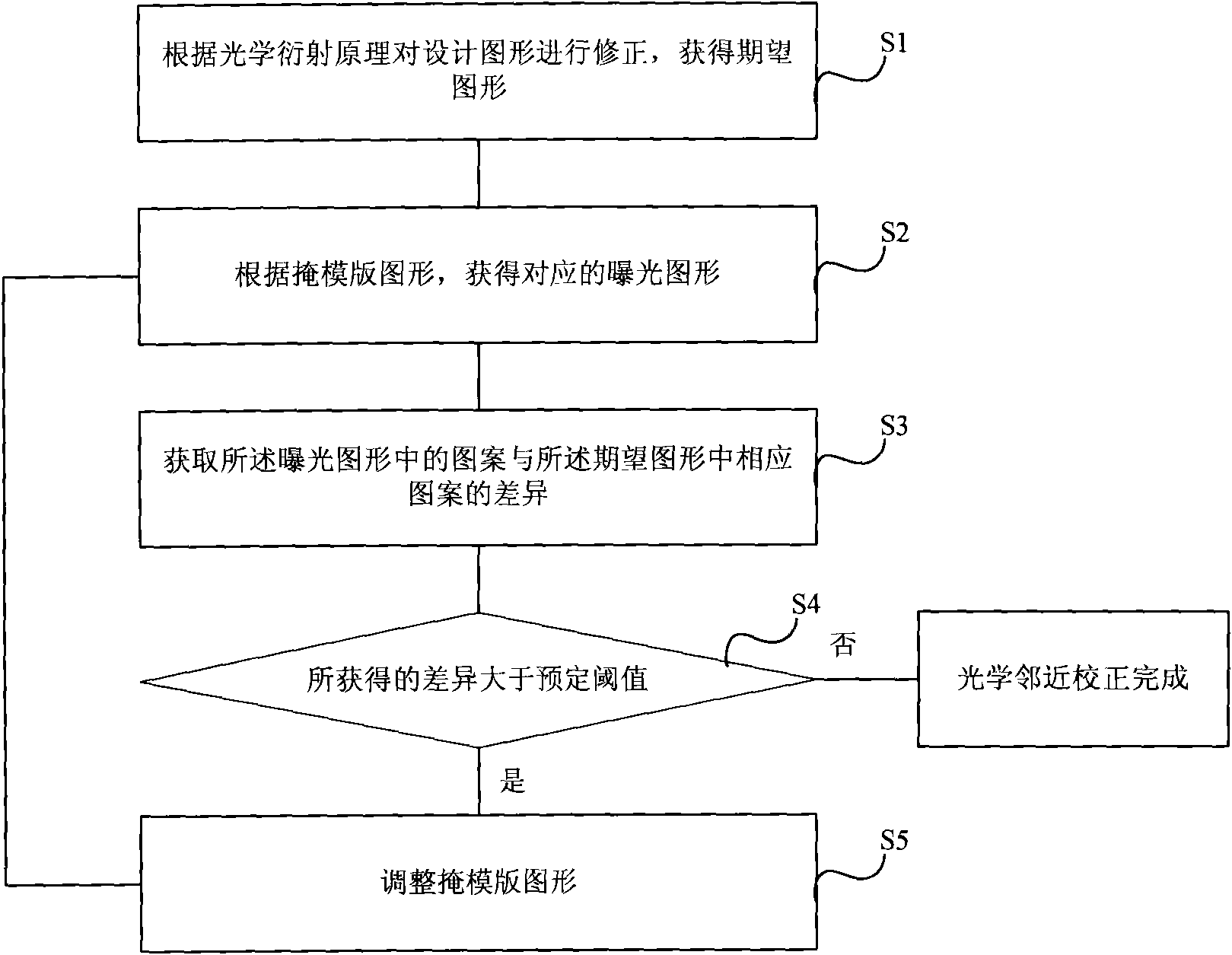
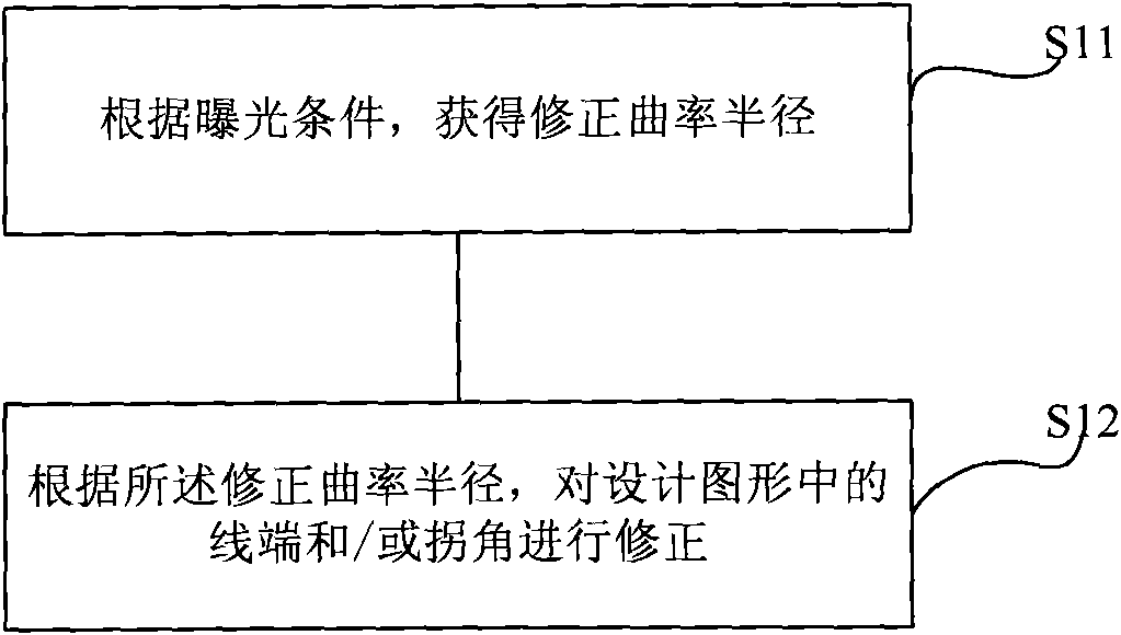
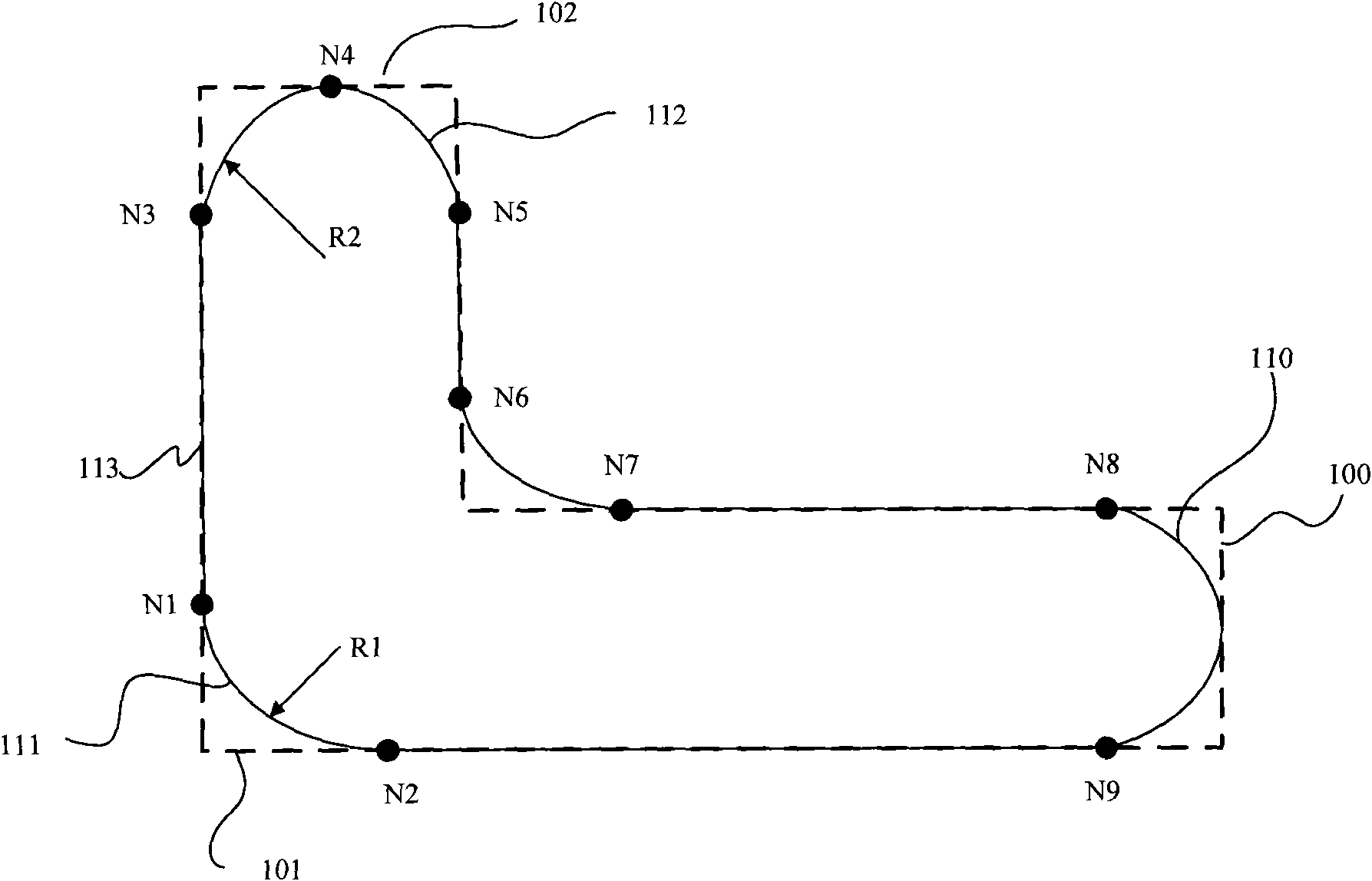
[0016] In a conventional optical proximity correction method, a better reticle pattern is obtained by repeatedly calculating the distance between the exposure pattern and each edge of the design pattern and comparing the distance with a predetermined threshold. However, due to the existence of the optical diffraction effect, the light diffraction effect is particularly obvious at the positions where the figures are adjacent to each other, especially at the top of the line segment and the corner of the figure. Based on the above phenomenon, after a lot of experiments and research, the inventor proposes the optical proximity correction method of the present invention, corrects the outline of the design figure according to the principle of optical diffraction to obtain the desired figure, and then compares the exposure figure with the desired figure instead of the design figure For comparison, the distance between corresponding edges in the two is calculated, and the distance is c...


PUM


Abstract

The invention relates to an optical proximity correction method which comprises the following steps: correcting a design figure according to the optical diffraction theory to acquire an expected figure; acquiring a corresponding exposure figure according to a mask plate figure; acquiring the difference between the pattern in the exposure figure and the corresponding pattern in the expected figure; comparing the acquired difference with the preset threshold; when the difference is less than or equal to the preset threshold, finishing the optical proximity correction; and when the difference is greater than the preset threshold, adjusting the mask plate figure, and carrying out the steps of exposing, computing and comparing again on the new mask plate figure until the optical proximity correction is finished. In the method of the invention, the time of the optical proximity correction is shortened and the production efficiency is improved.

Description

technical field [0001] The present invention relates to photolithography, and in particular to optical proximity correction methods. Background technique [0002] With the development of integrated circuits, the design size is getting smaller and smaller. Due to light diffraction and interference phenomena, there are certain deformations and deviations between the exposure pattern actually formed on the silicon wafer and the mask pattern. In the photolithography process, firstly, according to the design pattern, a mask plate is made, and the mask plate has a corresponding mask plate pattern; then, the mask plate is exposed, and the exposure light is projected on each layer of material of the silicon wafer through the mask plate, forming Exposure pattern associated with mask pattern. According to the principle of light wave diffraction and interference, light waves will diffract when passing through the mask, and light waves at different positions of the mask will also inter...

Claims


Application Information

Patent Timeline
IPC IPC(8): G03F1/14G03F1/36
Inventor 周从树
Owner STATE GRID CORP OF CHINA
Why Eureka
Try Eureka