Method and device for the detection of defects in an object

A technology for objects and defects, applied in the field of devices implementing the method, can solve the problems of hindering defect detection, unreliability, etc., and achieve the effect of avoiding detection of direct transmitted light and primary reflected light, and saving costs

Active Publication Date: 2011-04-06
GP INSPECT
View PDF11 Cites 5 Cited by
  • Summary
  • Abstract
  • Description
  • Claims
  • Application Information

AI Technical Summary

Problems solved by technology

[0003] However, in inhomogeneous objects, defects can sometimes only be detected in a very unreliable manner, since the presence of inhomogeneities prevents the detection of defects

Method used


Image

  • Method and device for the detection of defects in an object
  • Method and device for the detection of defects in an object
  • Method and device for the detection of defects in an object

Examples


Embodiment Construction

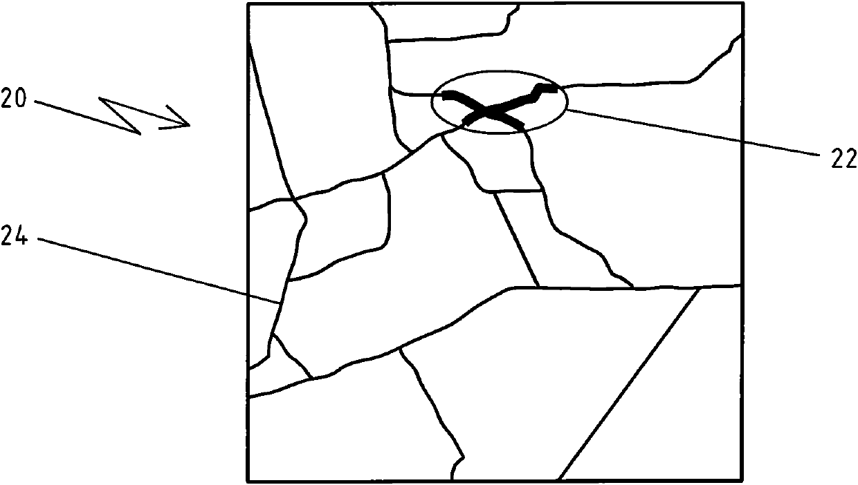
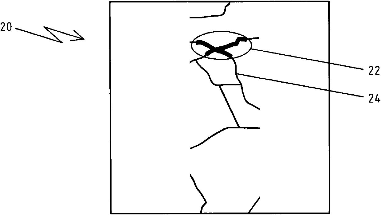
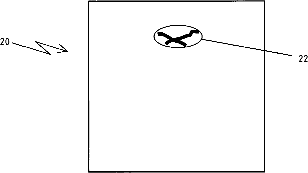
[0050] Figure 4 A first embodiment of the method according to the invention is shown in conjunction with a schematic diagram. According to this first embodiment, the polysilicon body is locally irradiated with infrared light (step 10). Furthermore, the light is detected (step 12) in a detection region which is spaced apart from an irradiation region in which the silicon body is locally irradiated and an exit region in which the silicon body is locally irradiated in order to locally irradiate The infrared light incident on the body is directly transmitted from the exit area. In this way, the detection of the direct transmission of the incident infrared light or the detection of the primary reflection of the infrared light can be largely avoided. As mentioned above, residual defects, in particular cracks or inclusions, can be identified using characteristic intensity differences in the detected portion of the incident light. Thus, analyzing this intensity difference, and in ...


PUM


Abstract

Method for detecting defects (22) in an object (20) comprising the steps of locally illuminating (10) the object (20) by radiating in light (50) having a wavelength to which the object (20) is transparent, detecting (12) multiply reflected components of the incident light (50) whilst at least partly avoiding the detection of directly transmitted components (48) of the incident light and at least partly avoiding the detection of singly reflected components (53a, 53b) of the incident light (50), and identifying (14) defects (22) by evaluating intensity differences in the detected components of the incident light (50), and device for carrying out the method.

Description

technical field [0001] The invention relates to a method for detecting defects in objects and to a device for carrying out the method. Background technique [0002] When manufacturing a product, an effort is usually made to produce as few defective parts as possible. The aim is therefore to check raw materials or semi-finished products for possible defects or defects before they go into production. In this way, defective raw materials or semi-finished products can be prevented from entering the manufacturing process and the resulting costs and expenditures until the final inspection or until the manufactured product is determined to be defective later. For example, silicon wafers are used as starting material in the production of semiconductor components, in particular solar cells. Wafers of silicon, often described as silicon wafers, with a thickness of up to a few hundred micrometers, are relatively thin and therefore brittle. When such silicon wafers enter the correspo...

Claims


Application Information

Patent Timeline
Patent Type & Authority Applications(China)
IPC IPC(8): G01N21/88
CPCG01N21/9501G01N21/9505H01R39/32H02K13/04B60P1/4492G01N2021/845
Inventor 马克·赫姆森道夫克里斯蒂安·普罗布斯特
Owner GP INSPECT
Why Eureka
Try Eureka