Level shift circuit, and driver and display device using the same

A level shifting circuit and circuit technology, which is applied in the direction of logic circuit connection/interface layout, logic circuit, logic circuit coupling/interface using field effect transistors, etc., which can solve the difficulty of saving area, complex circuit, large number of components, etc. problem, to achieve the effects of suppressing through current, suppressing duty cycle deterioration, and low power consumption

Inactive Publication Date: 2011-04-06
RENESAS ELECTRONICS CORP
View PDF5 Cites 1 Cited by
  • Summary
  • Abstract
  • Description
  • Claims
  • Application Information

AI Technical Summary

Problems solved by technology

[0009] in reference to Figure 11 , Figure 12 In the level shift circuit described above, although it is possible to increase the speed of level shifting, there are problems in that the circuit is complex, the number of elements is large, and area saving is difficult due to the fact that the self-resetting part contains many elements.

Method used


Image

  • Level shift circuit, and driver and display device using the same
  • Level shift circuit, and driver and display device using the same
  • Level shift circuit, and driver and display device using the same

Examples


Embodiment 1

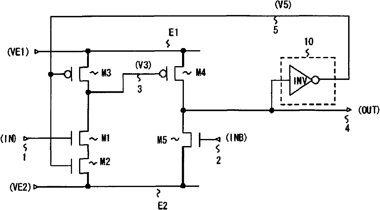
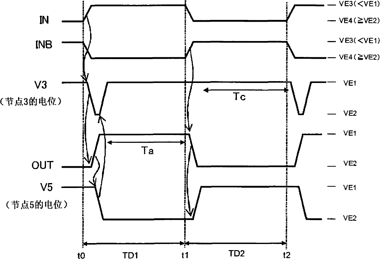
[0036] figure 1 is a diagram showing the structure of the first embodiment of the present invention. exist figure 1 Among them, IN and INB are complementary low-amplitude input signals having the amplitudes of the third and fourth voltage levels (VE3 and VE4). OUT is a high-amplitude output signal having amplitudes of the first and second voltage levels (VE1 and VE2). VE1 and VE2 are the first and second power supply voltages on the high potential and low potential sides. exist figure 1 Among them, the potential relationship of VE1, VE2, VE3, and VE4 is VE2≤VE4

[0037] refer to figure 1 , the level shift circuit of the first embodiment of the present invention has: a pMOS transistor M3 whose source is connected to the first power supply terminal (E1) supplying a first voltage level (VE1); an nMOS transistor M1 whose drain is connected to The drain of the pMOS transistor M3, the gate of which receives a low-amplitude input signal (IN); the nMOS transistor M2...

Embodiment 2

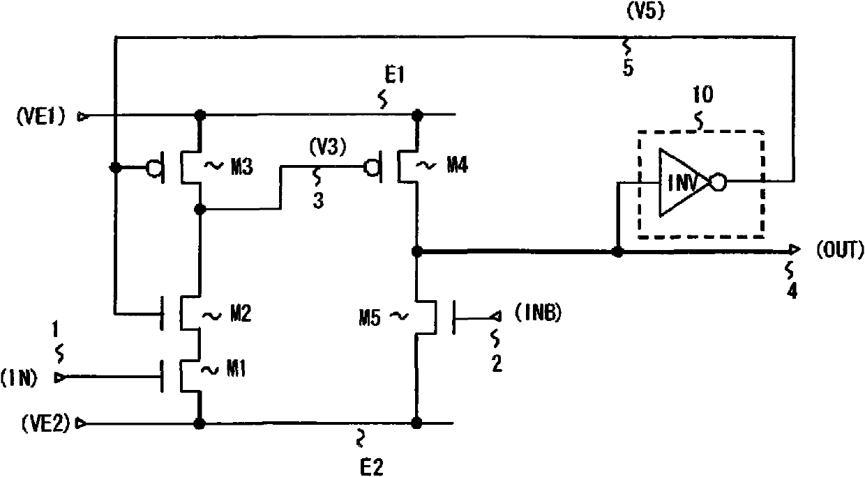
[0053] The second embodiment of the present invention will be described below. image 3 is a diagram showing the structure of the second embodiment of the present invention. refer to image 3 , in this example, swapping the figure 1 Connection of nMOS transistors M1, M2 in the shown structure. That is, the source of the nMOS transistor M1 whose gate receives the input signal IN is connected to the second power supply terminal (E2), and the nMOS transistor M2 whose gate receives the output 5 of the first delay circuit 10 is connected to the node 3 and the drain of the nMOS transistor M1 between poles. Also in this configuration, the same operation as that of the first embodiment described above is performed.

Embodiment 3

[0055] Next, a third embodiment of the present invention will be described. Figure 4 is a diagram showing the structure of a third embodiment of the present invention. refer to Figure 4 , in the third embodiment of the present invention has an nMOS transistor M5 and an nMOS transistor M6 connected in series between the second power supply terminal E2 and the output terminal 4 . and figure 1 Same as the first embodiment, the drain of the nMOS transistor M5 is connected to the output terminal 4, and the gate receives the input signal INB. The drain of the nMOS transistor M6 is connected to the source of the nMOS transistor M5, the source is connected to the second power supply terminal E2, and the gate receives a delayed signal in phase with the output signal OUT. In addition, as in the first and second embodiments, the connection order of the nMOS transistors M1 and M2 may be switched in this embodiment as well.

[0056] In addition, this embodiment also shows as a prefe...


PUM


Abstract

The invention provides a level shift circuit, and a driver and a display device using the same. The level shift circuit includes a first circuit connected between a first power supply terminal (PST) and an output terminal (OT) of the level shift circuit to set OT to a first voltage (V1) when conducting, a second circuit connected between a second PST and OT to set OT to the second voltage (V2) when conducting, and a third circuit that receives an input signal and a feedback signal from OT so that, when OT=V2 and input=a third voltage (V3), the first circuit conducts, and when OT=V1, the first circuit is made nonconductive irrespective of the value of the input signal. The second circuit is made conductive and nonconductive when the reverse-phase signal of the input signal is equal to V3 and the reverse-phase signal of the input signal is equal to a fourth voltage (V4), wherein V2<=V4<V3<V1.

Description

technical field [0001] The invention relates to a level shift circuit, a driver and a display device using the circuit. Background technique [0002] Recently, in the field of display devices, displays using various display devices, such as displays using liquid crystal display devices and organic EL elements, have been developed. These display devices tend to require higher image quality (multiple gradation) and higher voltage amplitudes of scanning signals and gradation signals. Therefore, it is required to increase the voltage of each output unit of a row driver that drives the scanning lines of the display panel and a column driver that drives the data lines of the display panel using grayscale signals. [0003] On the other hand, various control signals and image data signals supplied from the display controller to the row driver (scan driver) and column driver (data driver) require high-speed transmission and low EMI (Electromagnetic Interference: Electromagnetic Inte...

Claims


Application Information

Patent Timeline
Patent Type & Authority Applications(China)
IPC IPC(8): H03K19/0175H03K19/0185H03K17/16G09G3/20G09G3/36G09G3/30
CPCG09G2310/027H03K19/018521G09G2310/0289G09G3/20
Inventor 土弘
Owner RENESAS ELECTRONICS CORP
Why Eureka
Try Eureka