Electrostatic protection structure-containing circuit board
An electrostatic protection and circuit board technology, applied in emergency protection circuit devices, static electricity, emergency protection circuit devices for limiting overcurrent/overvoltage, etc. and other problems to achieve the effect of solving electrostatic protection
- Summary
- Abstract
- Description
- Claims
- Application Information
AI Technical Summary
Problems solved by technology
Method used
Image
Examples
Embodiment 1
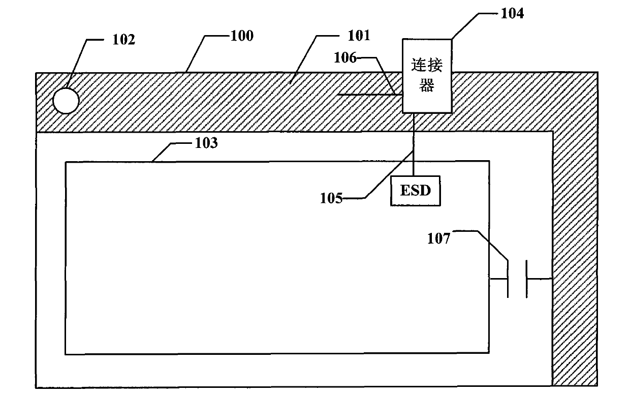
[0032] Refer to figure 1 , A circuit board 100 with an electrostatic protection structure, including a connector 104, the circuit board 100 includes a connecting hole 102, a protective ground area 101 (the shaded part in the figure) and a working ground area 103;
[0033] The protective ground area 101 is arranged on the two edges of a surface of the circuit board 100 and is arranged outside the working ground area 103 with a certain gap between the two; wherein, the protective ground area 101 is A copper skin layer with a certain width, the width can be 2mm, 3mm, 5mm, 1cm, etc. The width of the copper skin layer can be set according to the size of the circuit board, and the width can be set on the two edges of the circuit board.
[0034] The gaps can be set regularly, so that the distance between each part of the protected area 101 and the working area 103 is equal, that is, the gap has the same width, for example, the gap is a regular ring; or The gaps can be set irregularly, so ...
Embodiment 2
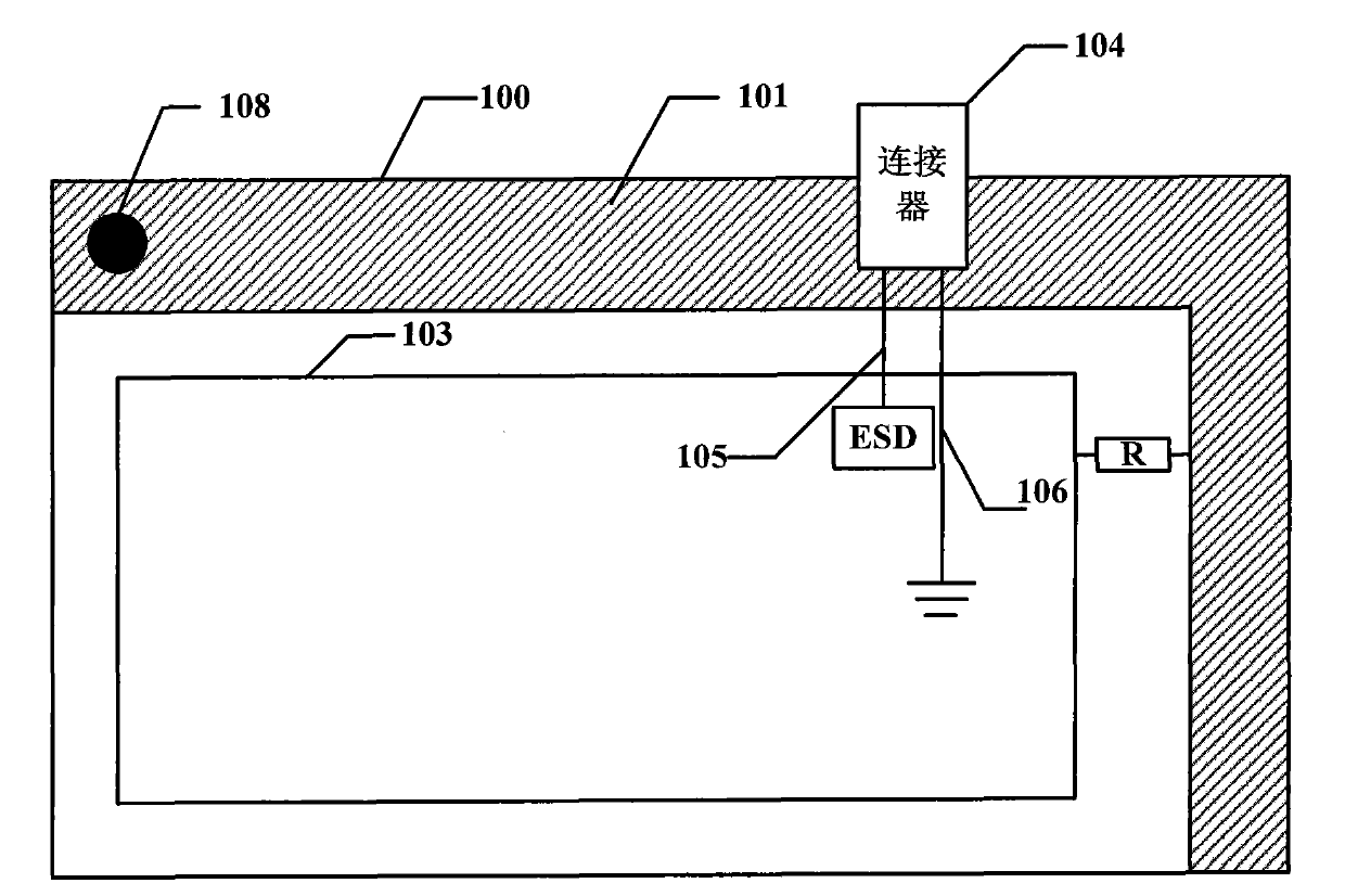
[0043] Refer to figure 2 In this embodiment, on the basis of embodiment 1, the circuit board 100 and the other circuit boards adopt a common ground connection mode, that is, the ground wire of the working ground area 103 of the circuit board 100 is connected to the other external circuit boards. The ground wire has a common ground terminal.
[0044] In addition, in the protected area 101, there is a solder joint 108 for guiding the static electricity of the protected area 101 into the ground. Wherein, in the gap between the protective ground area 101 and the working ground area, a varistor is connected to discharge the static electricity of the working ground area 103 to the protective ground area.
[0045] In this embodiment, the ground terminal of the connector 104 is connected to the ground terminal of the working ground area 103, and the signal line is connected with an ESD electrostatic protection device.
[0046] The rest is the same as the principle of Embodiment 1, and will...
Embodiment 3
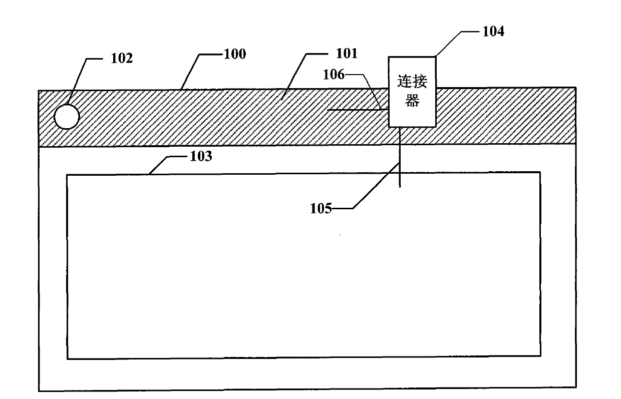
[0049] Refer to image 3 In this embodiment, on the basis of embodiment 1, the protective ground area 101 is only plated on one edge of the circuit board 100, and the signal line end of the connector 104 is not connected to an electrostatic protection device. And no discharge circuit is installed between the protective ground area 101 and the work ground area 103. Wherein, the cable of the connector 104 is a cable containing a conductive layer, and one end of the conductive layer of the cable is connected to the protective ground area 101. The connection method can be welding, lap connection or snap connection.
[0050] The rest is the same as in Embodiment 1, and will not be repeated here.
[0051] The solution of this embodiment can still effectively prevent the connector from bringing external static electricity into the circuit board.
PUM
 Abstract
Description
Claims
Application Information


