
Optical module mounting construction

An installation structure, optical module technology, applied in the direction of electrostatic, non-printed electrical components connected printed circuits, electrical components, etc., can solve the problem that the optical module provides a large metal plane, can not provide low-impedance electrostatic current discharge channels, etc. problems, to achieve the effect of meeting the requirements of electrostatic protection and overcoming technical prejudice

Active Publication Date: 2011-04-06
ZTE CORP
View PDF0 Cites 0 Cited by
  • Summary
  • Abstract
  • Description
  • Claims
  • Application Information

AI Technical Summary

Problems solved by technology

However, since this structural design cannot provide a large metal plane for the optical module, nor can it provide a low-impedance electrostatic current discharge channel, it brings a difficult problem of electrostatic protection for the optical port. Therefore, it has not yet appeared to install the optical module in This structure on PCB plastic panel

Method used


Image

  • Optical module mounting construction
  • Optical module mounting construction
  • Optical module mounting construction

Examples


Embodiment 1

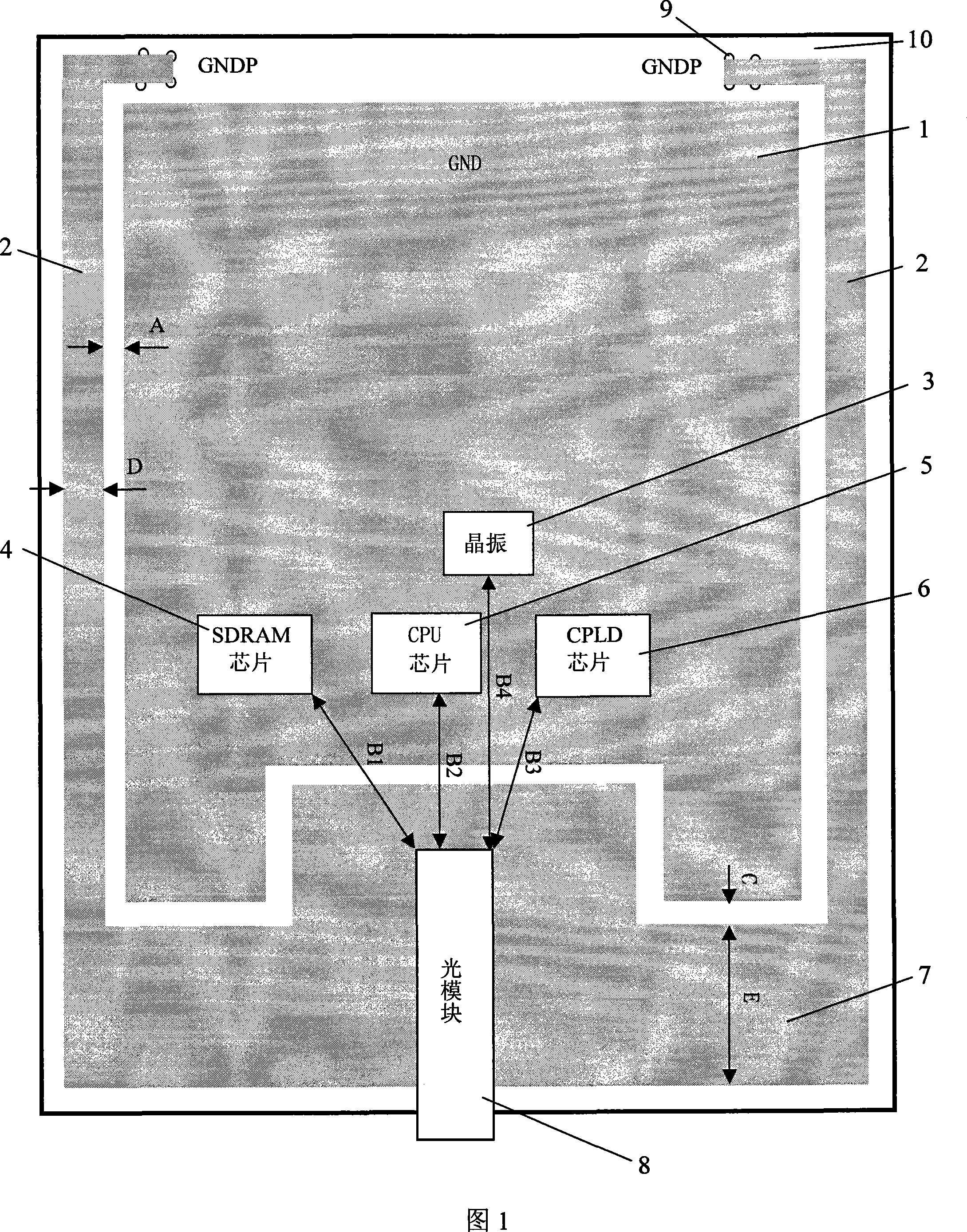
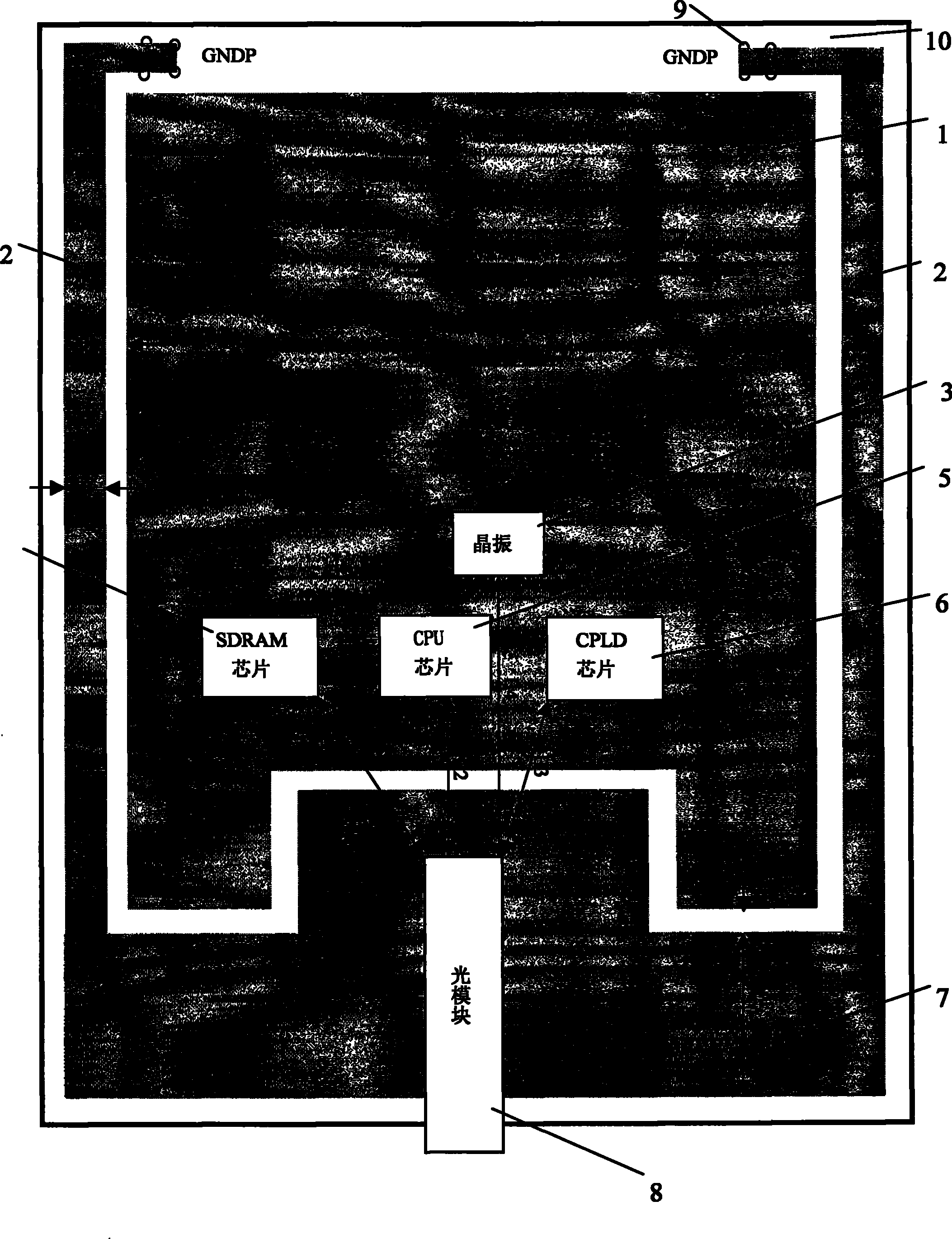
[0023] As shown in Figure 1, the optical module mounting structure of the present invention comprises a PCB board 10 and an optical module 8 installed on the PCB board 10, the layers of the PCB board can be double or multi-layered, in the area where the optical module 8 is located (including Each PCB layer (except the signal layer) on the edge of the circuit board) is designed as an optical module grounding area 7, and a certain number of vias (not shown in the figure) are set in the grounding area 7 along the edge and middle of the optical module grounding area. , the position and spacing of the via holes are adapted to the positions of the pins of the metal shell of the optical module. Usually, the distance between two via holes is about 2 cm. The optical module 8 is electrically connected to the grounds of these layers through the pins of the metal shell. On the side edge of each layer on the PCB board 10 where the optical module 7 is located, the PCB printed line 2 is laid ...

Embodiment 2

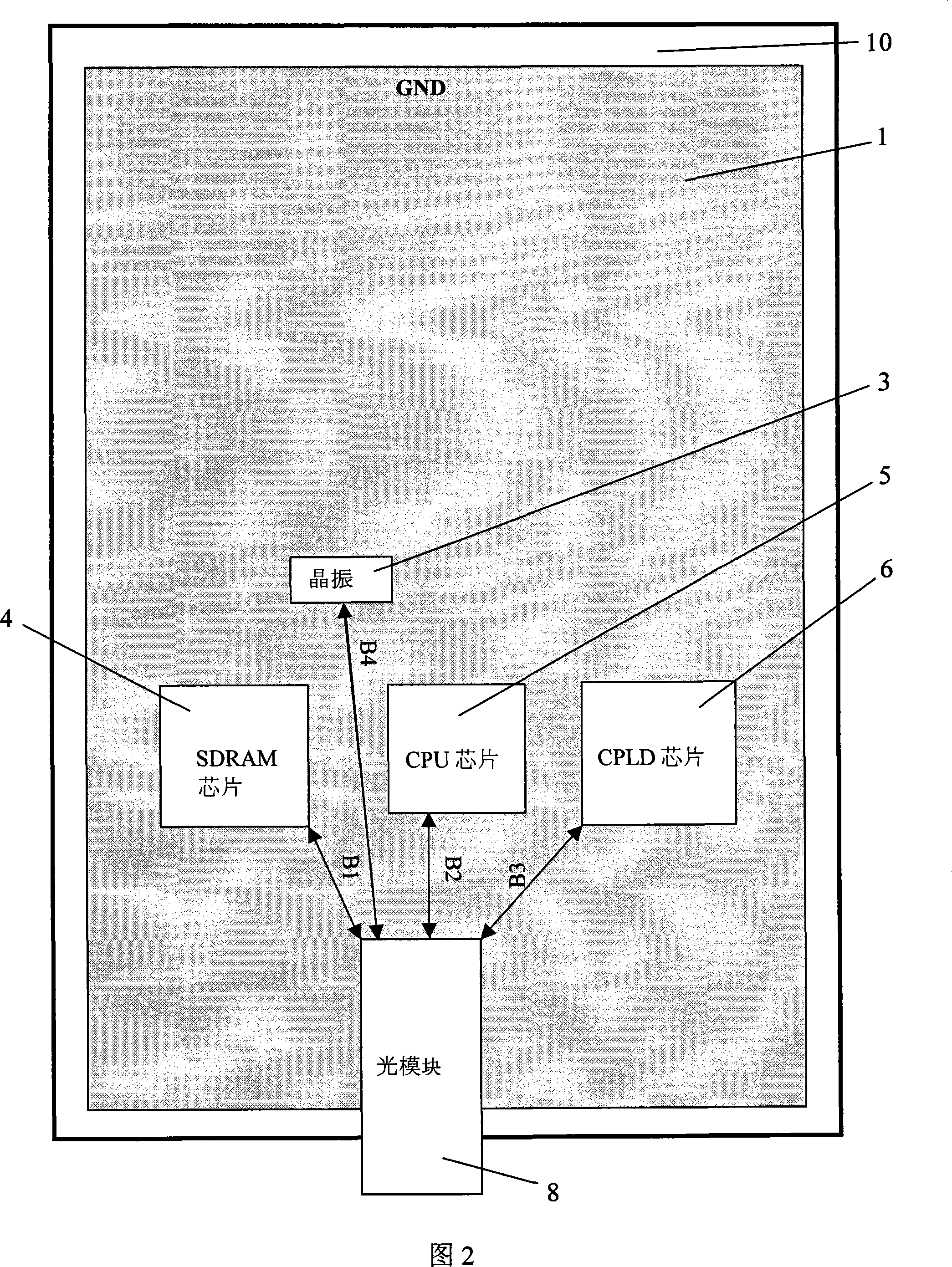
[0029] As shown in Figure 2, in this embodiment, the working ground 1 of the PCB board 10 is directly used as the ground of the shell metal pin of the optical module 8, and the key devices on the PCB board 10 are such as the CPU chip 5, the CPLD chip 6, the SDRAM chip 4, The minimum distance (B1, B2, B3, B4) between the crystal oscillator 3 and the metal housing of the optical module is 3 centimeters, so that the static electricity on the optical module 8 causes fluctuations in the working place to be insufficient to affect the normal operation of the above-mentioned chips. Tests have shown that it is more reasonable for the minimum distance to be 3 cm to 5 cm.

[0030] This embodiment is considered to be unreasonable and not allowed in traditional design. But for the optical port, there is no problem of lightning protection or EFT interference, so it is feasible to use the working ground on the circuit board as the static discharge ground of the optical module. Through the d...


PUM


Abstract

The invention relates to an optical module installing structure comprising a PCB board and an optical module which is arranged on the PCB board, the PCB board comprises ground on which the optical module is arranged, a outer metallic shell of the optical module is electrically connected with the ground which the optical module is arranged, and the minimum distance from the outer metallic shell ofthe optical module to a CPU chip, a CPLD chip, a SDRAM chip and a crystal oscillator chip on the PCB board is greater than or equal to 3cm. The optical module installing structure solves the static electricity protection problem of installing the optical module on a PCB plastic panel and ensures an optical interface to pass the EMS static electricity test; meanwhile, for a certain circuit board which has great intensity and can not guide and connect the ground of the optical module onto a protective ground GNDP of a system, the outer metallic shell of the optical module is connected with the working ground of the PCB board, thereby breaking the conventional design, overcoming the technical prejudice and meeting the requirements for static electricity protection of the optical interface.

Description

technical field [0001] The invention relates to a PCB board structure, more specifically, relates to a mounting structure of an optical module mounted on a plastic panel on a PCB board. Background technique [0002] Passing the electromagnetic compatibility EMC standard is an important condition for communication products to enter the international market, and electrostatic immunity is one of the requirements of the EMC standard. [0003] The optical port is a common interface for communication products, and the optical module housing is a metal case. If the position installed in the system is touched, an electrostatic test must be carried out on the optical port according to the standard requirements. If the electrostatic protection design of the optical port is not good and fails to pass the standard test, it will not only affect the communication performance of the optical port and the performance and life of the communication product, but also affect the market access, m...

Claims


Application Information

Patent Timeline
Patent Type & Authority Patents(China)
IPC IPC(8): H05K1/18H05F3/02
Inventor 王福联
Owner ZTE CORP
Learn More