Method for manufacturing circuit board, circuit board and chip packaging structure

A manufacturing method and chip packaging technology, which are applied to circuits, printed circuit components, secondary processing of printed circuits, etc., can solve the problem of reducing the wiring area of ​​the double-layer circuit board 100, and the wiring density of the double-layer circuit board 100 cannot be improved or reduced. Double-layer circuit board 100 wiring flexibility and other issues to achieve the effect of improving wiring density

Active Publication Date: 2012-11-28
ADVANCED SEMICON ENG INC
View PDF5 Cites 0 Cited by
  • Summary
  • Abstract
  • Description
  • Claims
  • Application Information

AI Technical Summary

Problems solved by technology

However, these through holes 116 and 118 will reduce the routing area of ​​the double-layer circuit board 100 and reduce the wiring flexibility of the double-layer circuit board 100, and cause the wiring density of the double-layer circuit board 100 to be unable to increase.

Method used


Image

  • Method for manufacturing circuit board, circuit board and chip packaging structure
  • Method for manufacturing circuit board, circuit board and chip packaging structure
  • Method for manufacturing circuit board, circuit board and chip packaging structure

Examples


Embodiment Construction

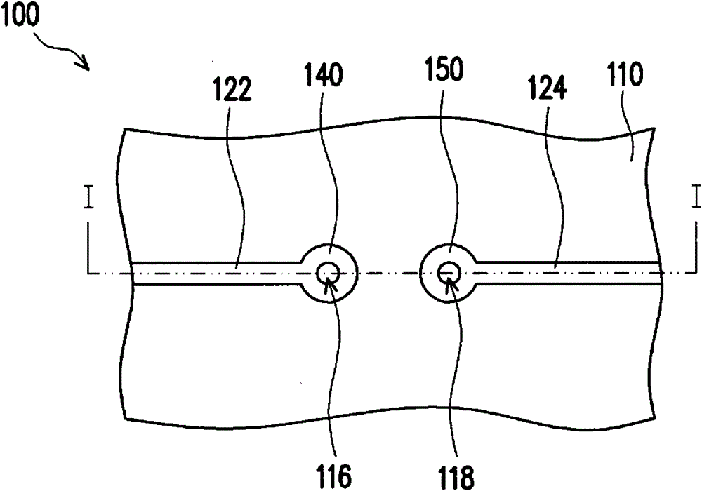
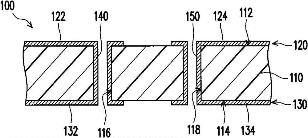
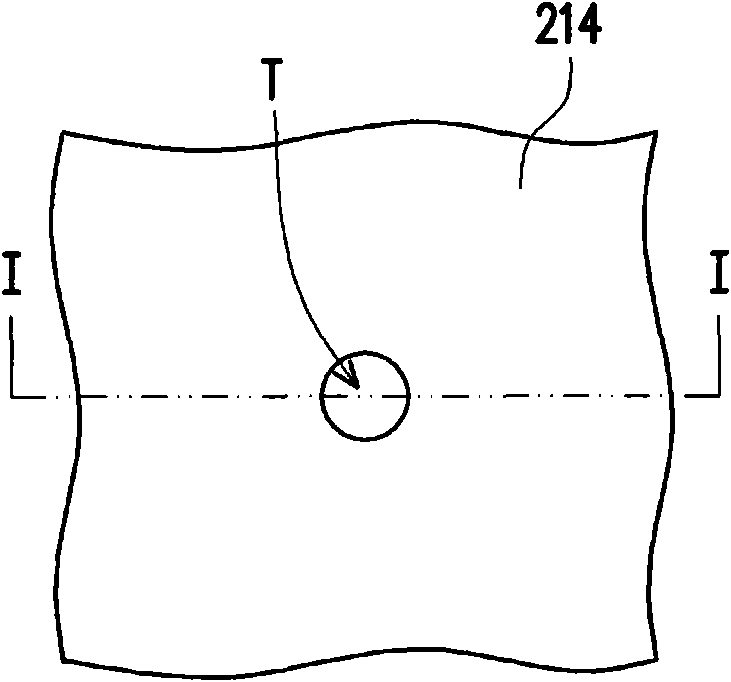
[0045] Figure 2A to Figure 2GIt is a top view of the manufacturing process of the circuit board according to an embodiment of the present invention. Figure 3A to Figure 3G respectively Figure 2A to Figure 2G The sectional view along the I-I line. Figure 4A to Figure 4E respectively Figure 2C to Figure 2G The sectional view along the line II-II. Figure 5A to Figure 5D respectively Figure 2D to Figure 2G Bottom view of the manufacturing process. It is worth noting that, Figure 2F only Figure 4C The top view of the middle area A, Figure 2G only Figure 4D Top view of middle area A.

[0046] Please refer to Figure 2A and Figure 3A , Firstly, a substrate 210 (such as a copper foil substrate) is provided, and the substrate 210 has a through hole T. In detail, the substrate 210 includes an insulating layer 212 , a first metal layer 214 and a second metal layer 216 , wherein the insulating layer 212 has a first surface 212 a and a second surface 212 b opposite ...


PUM


Abstract

The invention relates to a method for manufacturing a circuit board, the circuit board and a chip packaging structure. The method for manufacturing the circuit board comprises the following steps of: providing a substrate provided with a first surface and a second surface which are opposite; forming a through hole connecting the first surface and the second surface on the substrate; totally forming a conducting layer on the substrate; forming two grooves on the conducting layer, wherein the two grooves respectively extend to the second surface to divide the part of the conducting layer, whichis positioned in the through hole and at the periphery of the through hole, into a first conducting channel and a second conducting channel; and patterning the conducting layer, forming a first conducting path line and a second conducting path line on the first surface and forming a third conducting path line and a fourth conducting path line on the second surface. The method for manufacturing the circuit board, the circuit board and the chip packaging structure contribute to increasing the wiring area of the circuit board, improving wiring flexibility and improving the wiring density of the circuit board.

Description

technical field [0001] The invention relates to a circuit board and a manufacturing method thereof, in particular to a manufacturing method of a circuit board with high conductive trace density, a circuit board and a chip packaging structure. Background technique [0002] In circuit board technology, a conductive channel is an indispensable component of a circuit board. The conductive channel can pass through one or more insulating layers of the circuit board, and is used to connect two adjacent or non-adjacent circuit layers of the circuit board, so that the two circuit layers can be electrically connected to each other. [0003] Figure 1A It is a partial top view of a double-layer circuit board in the prior art, and Figure 1B for Figure 1A The cross-sectional view of the double-layer circuit board along the I-I line. Please also refer to Figure 1A and Figure 1B , the existing double-layer circuit board 100 includes an insulating layer 110 , two circuit layers 120 a...

Claims


Application Information

Patent Timeline
Patent Type & Authority Patents(China)
IPC IPC(8): H05K3/40H05K3/42H05K3/28H05K1/02H01L23/48H01L23/13
CPCH01L2224/16225H01L2224/32225H01L2224/73204H01L2924/15311
Inventor 黄士辅苏洹漳谢佳雄
Owner ADVANCED SEMICON ENG INC
Why Eureka
Try Eureka