Touch structure and touch display device
A touch display device and touch technology, which are applied in the fields of instruments, computing, electrical and digital data processing, etc., can solve the problems of increasing the complexity of the wiring design of the touch structure, so as to increase the routable area, reduce the frame area, The effect of reducing the wiring area
- Summary
- Abstract
- Description
- Claims
- Application Information
AI Technical Summary
Problems solved by technology
Method used
Image
Examples
Embodiment 1
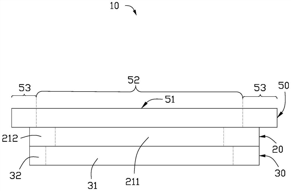
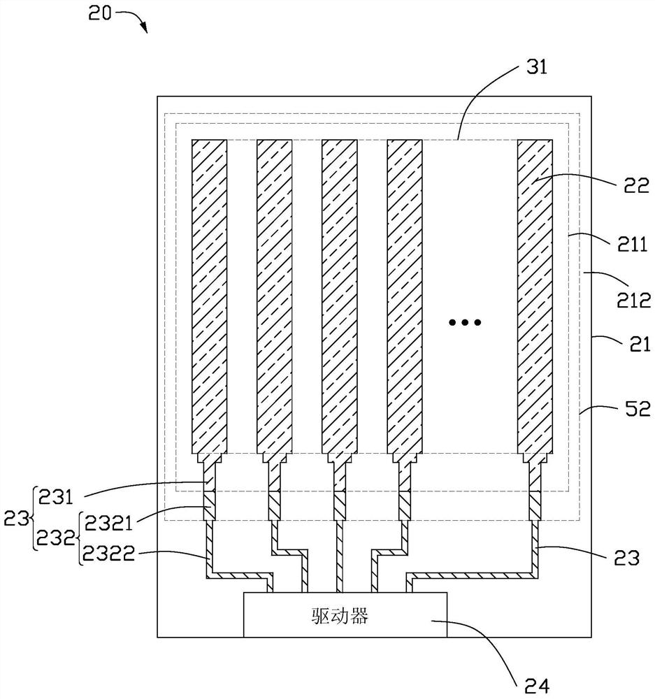
[0026] see figure 1 The touch display device 10 provided in this embodiment includes a touch structure 20 and a display panel 30 , and further includes a cover plate 50 located on a side of the touch structure 20 away from the display panel 30 . Wherein, in this embodiment, the touch structure 20 is stacked and disposed with the display panel 30 as a structure independent of the display panel 30 . In other embodiments, the touch structure 20 may be embedded in the display panel 30 , which is not correct in the embodiment of the present invention. The touch structure 20 and the structure of the display panel 30 are defined. The touch structure 20 is used for touch operation, the display panel 30 is used for image display, the surface 51 of the cover plate 50 away from the touch structure 20 is used as a touch surface during touch operation, and the surface 51 is also used for displaying the display panel 30 displayed images. The touch display device 10 provided in this embodi...
Embodiment 2
[0042] see Figure 5 The main difference between the touch control structure 40 provided in this embodiment and the first embodiment is that the second extending portion 432 is a double-layer structure of transparent conductive material and metal. Only the above differences will be described in detail below:
[0043] see Image 6 The second extension portion 432 of the electrical connection line 43 includes a stacked metal layer 4321 and a transparent conductive layer 4322 , wherein the transparent conductive layer 4322 is located between the substrate 41 and the metal layer 4321 . In this embodiment, the transparent conductive layer 4322 is made of the same material as the first extension portion 431 and the touch electrode 42 , which is indium tin oxide; the metal layer 4321 is copper.
[0044] The following will Image 6 The manufacturing process of the middle touch structure 40 is described as follows:
[0045] see Figure 7 , a base material 45 is formed on the subst...
PUM
 Abstract
Description
Claims
Application Information


