Semiconductor integrated circuit

a technology of integrated circuits and semiconductors, applied in the direction of generating/distributing signals, pulse techniques, instruments, etc., can solve the problems of increasing the area of semiconductor substrates, so as to prevent degradation of multiphase clock signal waveforms, the effect of increasing the wiring area of multiphase clock signals

Inactive Publication Date: 2007-01-02
THINE ELECTRONICS
View PDF5 Cites 10 Cited by
  • Summary
  • Abstract
  • Description
  • Claims
  • Application Information

AI Technical Summary

Benefits of technology

[0013]It is therefore an object of the present invention to provide a semiconductor integrated circuit that can prevent multiphase clock signals having the same phase difference, which signals are generated by a multi-stage differential ring oscillator and transmitted to other circuits, from being degraded in waveform due to electrostatic coupling between wirings thereof and that enables the multiphase clock signals to be wired in as small an area as possible.
[0015]According to the present invention, it is possible to prevent degradations of multiphase clock signal waveforms due to stray capacities without increasing the wiring area of the multiphase clock signals.

Problems solved by technology

This method, however, increases a wiring area for the multiphase clock signals.
This technique, however, requires an additional area for laying the new wirings, increasing the wiring area for the multiphase clock signals.
Hence, arranging wirings for the multiphase clock signals using the above-mentioned conventional technique requires a large wiring area, giving rise to a problem of an increased semiconductor substrate area.

Method used


Image

  • Semiconductor integrated circuit
  • Semiconductor integrated circuit
  • Semiconductor integrated circuit

Examples


Embodiment Construction

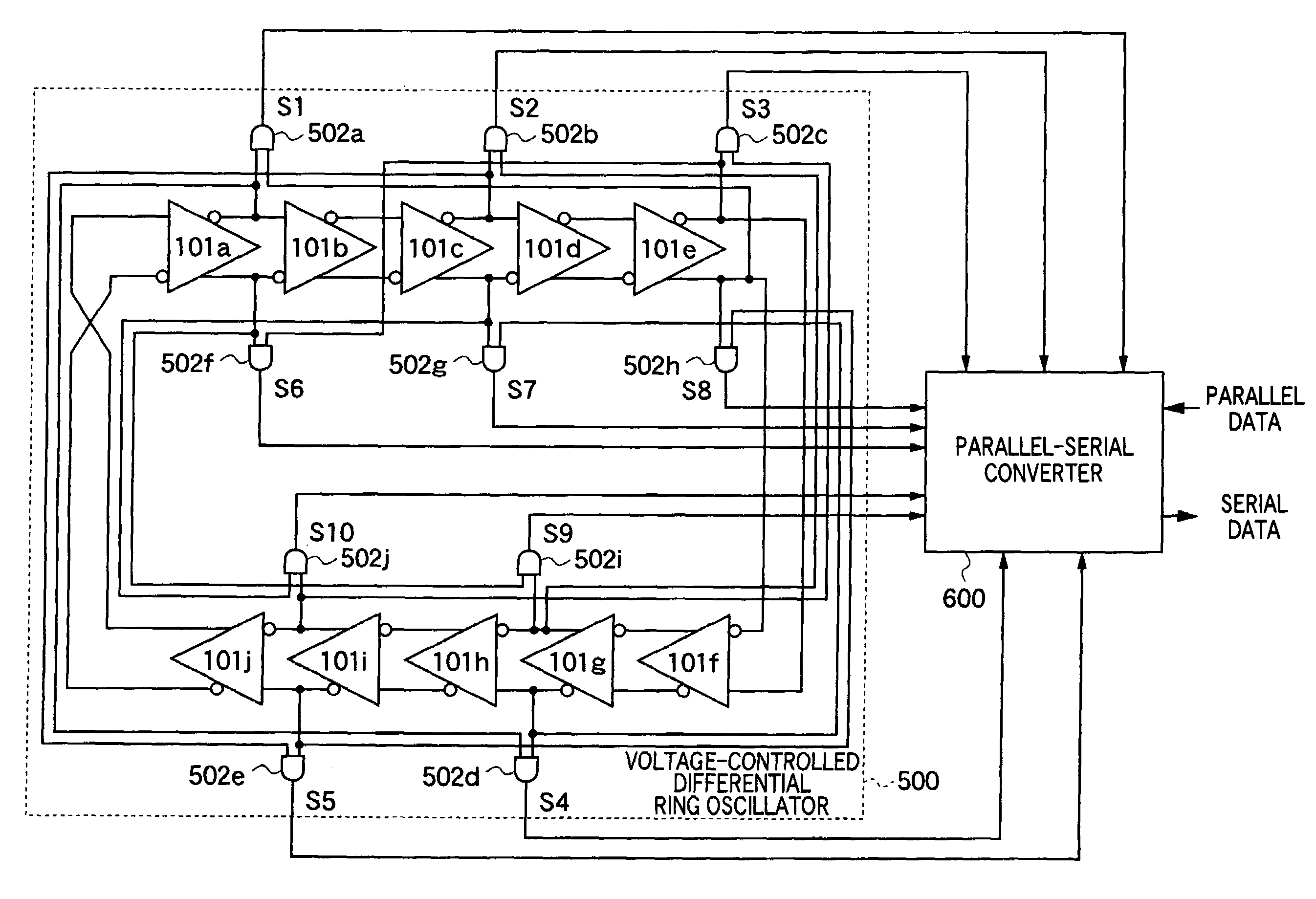
[0029]FIG. 5 shows a configuration of a semiconductor integrated circuit according to a first embodiment of the present invention. As shown in FIG. 5, this semiconductor integrated circuit includes a voltage-controlled differential ring oscillator 500 for outputting multiphase clock signals and a parallel-serial converter 600 for converting received parallel data into serial data on the basis of the multiphase clock signals. The parallel-serial converter 600 may be provided on the outside of the semiconductor integrated circuit.

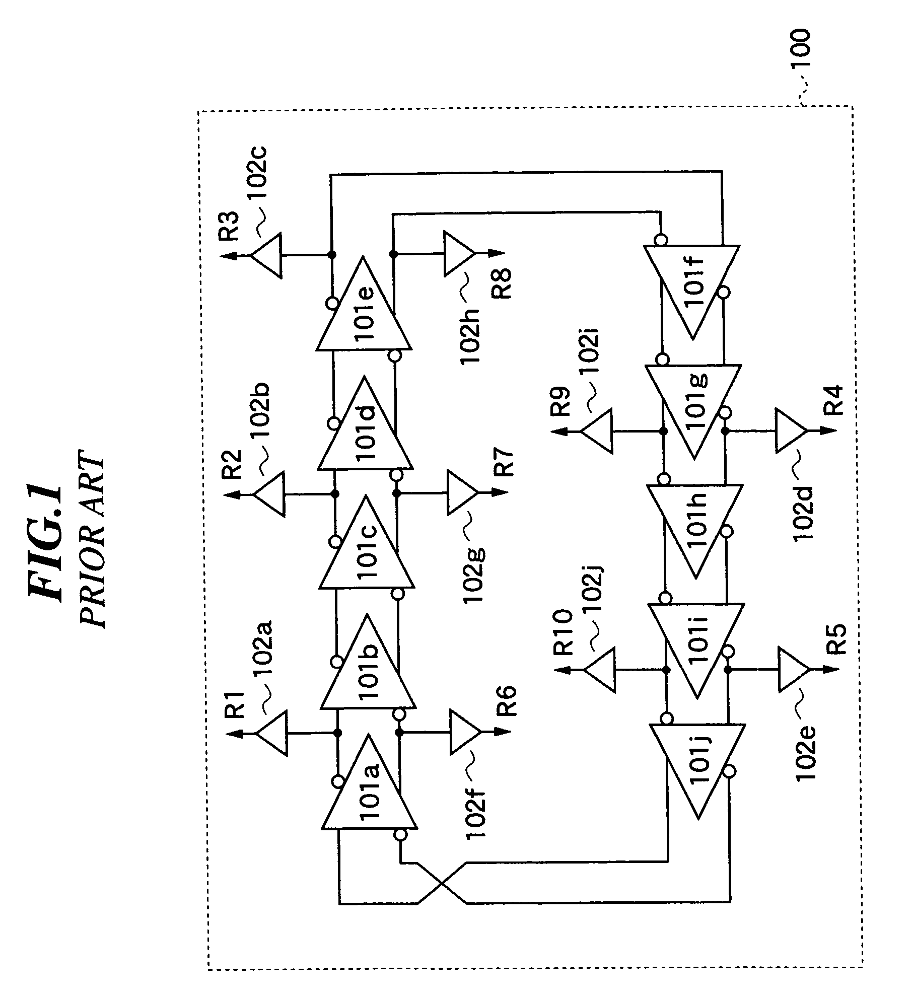
[0030]The voltage-controlled differential ring oscillator 500 includes N stages of delayed differential inverted amplifiers 101a, 101b, . . . for performing oscillating operation and logic circuits 502a, 502b, . . . for performing logic operation on the basis of output signals of the delayed differential inverted amplifiers 101a, 101b, . . . to output clock signals having M phases. Generally, it is preferred that N is a positive even number and M is an even n...


PUM


Abstract

A semiconductor integrated circuit in which multiphase clock signals having the same phase difference are supplied from a multi-stage differential ring oscillator to other circuits, the multiphase clock signals can be prevented from being degraded in waveform due to electrostatic coupling between wirings of the multiphase clock signals and also wired in as small an area as possible. The semiconductor integrated circuit includes: multiple stages of amplifier circuits, connected in a ring form, for performing oscillating operation; a logic circuit for performing logic operation on the basis of predetermined ones of output signals of the multiple stages of amplifier circuits to output a plurality of clock signals having different phases from each other and duties not equal to 0.5; and a plurality of wirings for transmitting the plurality of clock signals output from the logic circuit.

Description

[0001]This is a continuation of application Ser. No. 10 / 333,010 filed Jan. 15, 2003 now abandoned. The entire disclosure of the prior application, application Ser. No. 10 / 333,010 is hereby incorporated by reference.TECHNICAL FIELD[0002]The present invention relates generally to a semiconductor integrated circuit and more particularly to a semiconductor integrated circuit including a differential ring multiphase oscillator.BACKGROUND ART[0003]For signal transmission among devices, a technique employing high-speed and small-amplitude serial signals has been in use in recent years. Compared with a technique that transmits digital signals in parallel, this technique needs only a small number of cables and also can minimize electromagnetic interference (EMI) caused by the digital signal transmission.[0004]To realize a high-speed serial communication, a parallel-serial converter is required on a transmit side which converter converts parallel data into serial data by using sub-clock signa...

Claims


Application Information

Patent Timeline
Patent Type & Authority Patents(United States)
IPC IPC(8): G11C8/00G11C7/00G06F1/06G06F1/10H03K3/0231H03K3/03H03K5/15
CPCG06F1/10H03K3/0322H03K3/03H03K3/0231
Inventor OKAMURA, JUNICHI
Owner THINE ELECTRONICS
Why Eureka
Try Eureka