Semiconductor device, manufacturing method thereof, display device, and electronic device
Active Publication Date: 2018-05-03
SEMICON ENERGY LAB CO LTD
View PDF15 Cites 5 Cited by
Summary
Abstract
Description
Claims
Application Information
AI Technical Summary
This helps you quickly interpret patents by identifying the three key elements:
Problems solved by technology
Method used
Benefits of technology
Benefits of technology
This patent describes a novel semiconductor device that has high data transmission capacity. This is achieved by increasing the number of wirings and transmitting signals in parallel. This method can be used in display devices with increased image data, such as full high-definition and ultra-high-definition display devices. The semiconductor device allows for efficient data transmission with a small number of wirings. Overall, this invention provides a solution for high-speed data transmission in electronic devices.
Problems solved by technology
However, this method causes, for example, increases in the number of input / output terminals, the power consumption, and the semiconductor chip size.
Method used
Image
Click on the blue label to locate the original text in one second.
Reading with bidirectional positioning of images and text.
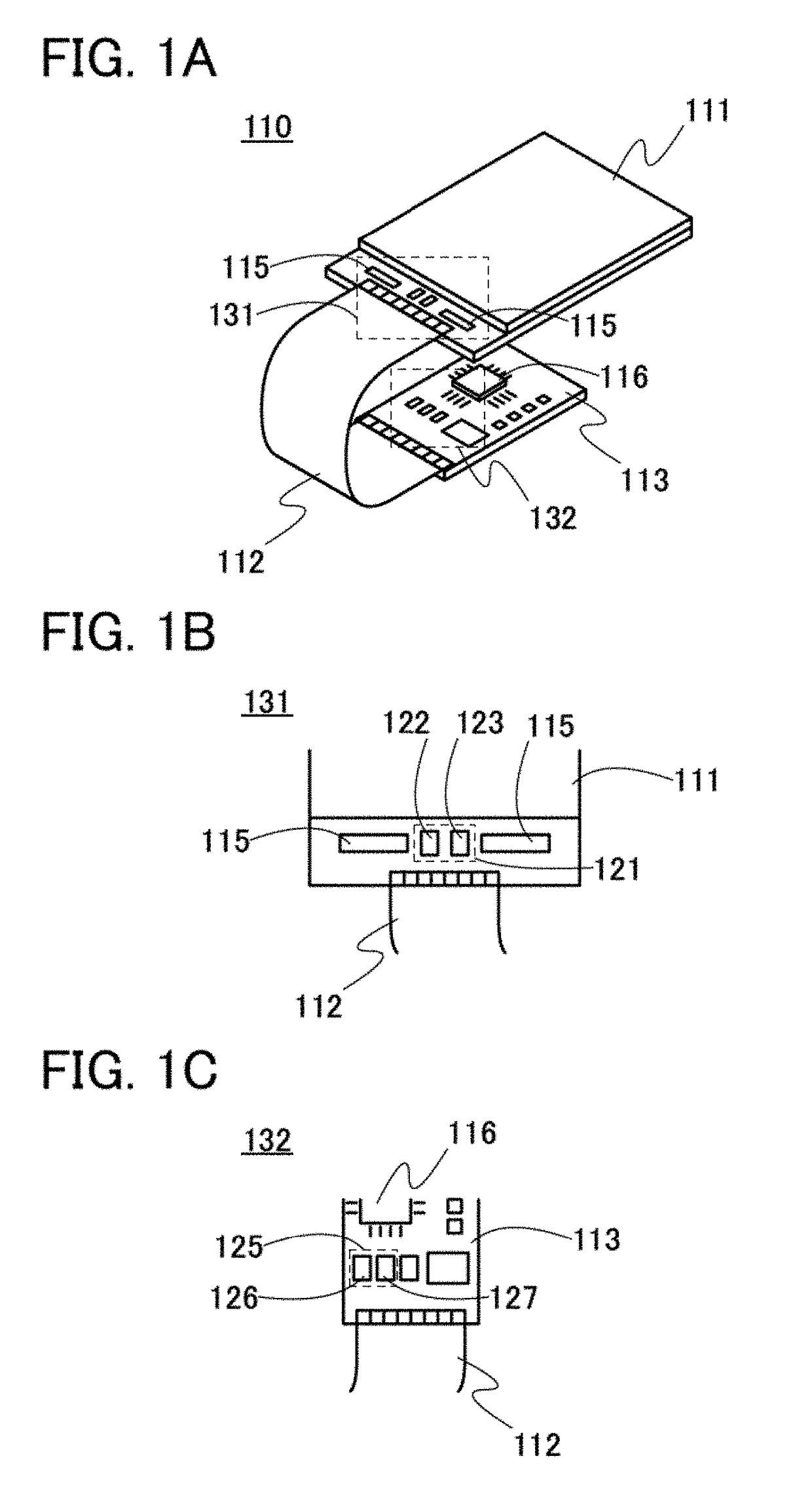
[0086]FIG. 1A is a perspective view illustrating a structural example of a semiconductor device 110. FIG. 1B is a top view illustrating a structure around a region 131, and FIG. 1C is a top view illustrating a structure around a region 132.
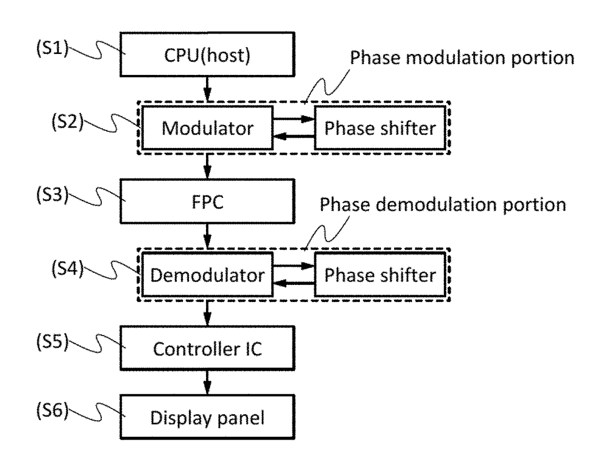
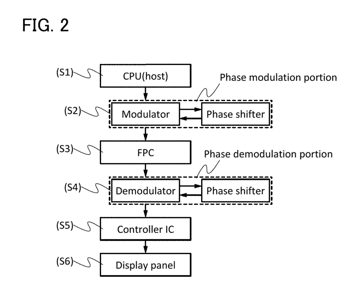
[0087]The semiconductor device 110 shown in FIGS. 1A to 1C includes a display panel 111, an FPC 112, a substrate 113, a controller IC 115, a phase demodulation portion 121, a phase modulation portion 125, and a CPU 116.
[0088]The CPU 116 in an electronic device such as a mobile phone or a laptop PC has a function of processing information and generating image data. The function of generating image data is not necessarily unique to the CPU, and a graphicsprocessing unit (GPU) may generate image data, for example. What generates image data changes depending on electronic devices; ...
embodiment 2
[0178]In this embodiment, examples of the display panel 111 described in Embodiment 1 is described with reference to FIG. 10, FIGS. 11A1, 11A2, and 11B, and FIGS. 12A1, 12A2, and 12B.
[0179]FIG. 10 is a schematic perspective view of the display panel 111. The display panel 111 includes a display region 935, a peripheral circuit region 901, and a wiring 965 that are over a substrate 951. FIG. 10 shows an example where the controller IC 115, the phase shifter 122, the demodulator 123, and the FPC 112 are mounted on the display panel 111.
[0180]The peripheral circuit region 901 includes a circuit for supplying a signal to the display region 935. The circuit included in the peripheral circuit region 901 is, for example, a gate driver.
[0181]The wiring 965 has a function of supplying a signal and power to the display region 935 and the peripheral circuit region 901. The signal and power are input to the wiring 965 from the outside through the FPC 112 or from the controller IC 115.
[0182]In t...
embodiment 3
[0289]This embodiment will introduce a hybrid display panel that includes a light-emitting element and a reflective element as another example of the display panel 111 in Embodiment 1, and describe cross-sectional structure examples of the hybrid display panel.
Example 1 of Cross-Sectional Structure
[0290]FIG. 16 shows a cross-sectional structure example of the display panel 111. FIG. 16 illustrates an example of cross sections of a region including the FPC 112, a region 472 in the gate driver 313 or 314, and a region 471 in the pixel array 311.
[0291]The display panel 111 includes an insulating layer 420 between substrates 411 and 412. A light-emitting element 401, a transistor 403, a transistor 404, a transistor 405, a coloring layer 413, and the like are between the substrate 411 and the insulating layer 420. A liquid crystal element 402, a coloring layer 414, and the like are between the insulating layer 420 and the substrate 412. The substrate 412 and the insulating layer 420 are ...
PUM
Abstract
A method for transmitting image data to a display device at high speed is provided. Image data to be transmitted is input to a phase modulation portion, and is mixed with a high-frequency carrier wave. The carrier wave is modulated with a technique of phase-shift keying, and output to a transmission line determined in consideration of the transmission characteristics of the high-frequency wave. A phase regulating portion of the phase modulation portion has a function of adjusting the amount of change in phase with the use of an electric signal. A phase demodulation portion beyond the transmission line demodulates the modulated carrier wave and extracts the image data. The multi-bit image data can be transmitted by the technique of the phase-shift keying. The high-speed transmission enables serial conversion of the original image data and decreases the number of transmission lines.
Description
BACKGROUND OF THE INVENTION1. Field of the Invention[0001]One embodiment of the present invention relates to a semiconductor device.[0002]Note that one embodiment of the present invention is not limited to the above technical field. The technical field of the invention disclosed in this specification and the like relates to an object, a method, or a manufacturing method. Furthermore, one embodiment of the present invention relates to a process, a machine, manufacture, or a composition of matter.[0003]Specific examples of the technical field of one embodiment of the present invention disclosed in this specification and the like include a semiconductor device, a display device, an electronic device, a method for driving any of them, and a method for manufacturing any of them. In this specification and the like, a semiconductor device generally means a device that can function by utilizing semiconductor characteristics. For example, an integrated circuit, a chip including an integrated...
Claims
Application Information
Patent Timeline
Application Date:The date an application was filed.
Publication Date:The date a patent or application was officially published.
First Publication Date:The earliest publication date of a patent with the same application number.
Issue Date:Publication date of the patent grant document.
PCT Entry Date:The Entry date of PCT National Phase.
Estimated Expiry Date:The statutory expiry date of a patent right according to the Patent Law, and it is the longest term of protection that the patent right can achieve without the termination of the patent right due to other reasons(Term extension factor has been taken into account ).
Invalid Date:Actual expiry date is based on effective date or publication date of legal transaction data of invalid patent.

