Semiconductor device, manufacturing method thereof, display device, and electronic device

a technology of semiconductor chip and display device, which is applied in the direction of static indicating device, phase-modulated carrier system, instruments, etc., can solve the problems of increasing the number of input/output terminals, power consumption, and the size of semiconductor chips, so as to increase the image data, improve the image quality of the display device, and increase the image data

Active Publication Date: 2021-06-22
SEMICON ENERGY LAB CO LTD
View PDF21 Cites 0 Cited by
  • Summary
  • Abstract
  • Description
  • Claims
  • Application Information

AI Technical Summary

Benefits of technology

[0009]The image quality of a display device is improved by, for example, an increase in the number of pixels, the number of display colors, or the frame frequency, which increases the image data. A display device including both a reflective element and a light-emitting element has increased image data when the reflective element and the light-emitting element display different images. The increase in image data causes an increase in data amount transmitted between a controller of the display device in an electronic device and a host of the electronic device. An object of one embodiment of the present invention is to provide a semiconductor device that has high data transmission capacity.
[0010]A method for increasing the data transmission capacity is to increase the number of wirings and transmit signals in parallel. However, this method causes, for example, increases in the number of input / output terminals, the power consumption, and the semiconductor chip size. Thus, another object is to provide a semiconductor device that has high data transmission capacity with a small number of wirings.
[0011]For example, a display device with 1920×1080 pixels that is called a full high-definition (FHD) display device is employed in TVs, laptop PCs, smartphones, and the like. When image data for full high-definition display is transmitted by low-voltage differential signaling (LVDS) that is used for short-distance (several centimeters to approximately twenty centimeters) data transmission, 12 pairs of wirings (24 wirings) are required at a frame frequency of 60 Hz. Furthermore, a display device that has four times as much pixels as a FHD display device does, which is called an ultra-high-definition (4K2K) display device, is employed in part of TVs, laptop PCs, smartphones, and the like. Thus, another object is to provide a semiconductor device with high data transmission capacity that can transmit image data for these display devices with a small number of wirings.
[0044]According to one embodiment of the present invention, a novel semiconductor device can be provided. A novel semiconductor device with high data transmission capacity can be provided. A novel semiconductor device that has high data transmission capacity with a small number of wirings can be provided. According to one embodiment of the present invention, a novel display device can be provided.

Problems solved by technology

However, this method causes, for example, increases in the number of input / output terminals, the power consumption, and the semiconductor chip size.

Method used


Image

  • Semiconductor device, manufacturing method thereof, display device, and electronic device
  • Semiconductor device, manufacturing method thereof, display device, and electronic device
  • Semiconductor device, manufacturing method thereof, display device, and electronic device

Examples


embodiment 1

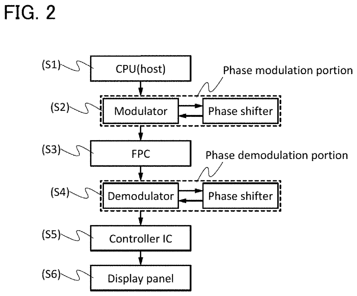
[0085]This embodiment will describe a semiconductor device including a phase modulation portion, an FPC, a phase demodulation portion, a controller IC, and a display panel.

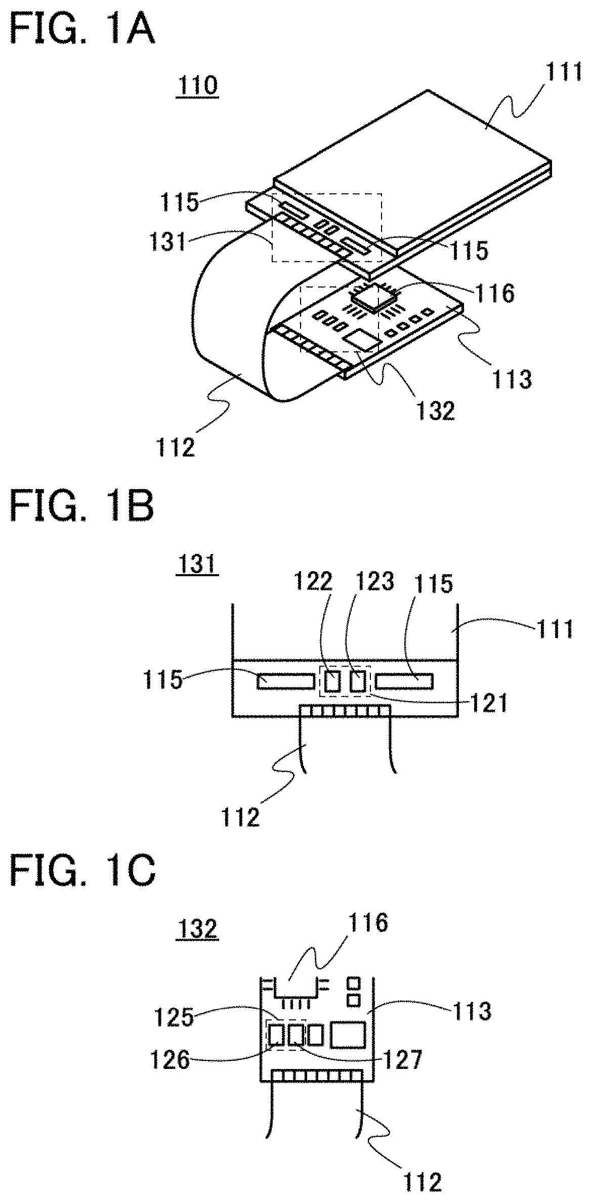
[0086]FIG. 1A is a perspective view illustrating a structural example of a semiconductor device 110. FIG. 1B is a top view illustrating a structure around a region 131, and FIG. 1C is a top view illustrating a structure around a region 132.

[0087]The semiconductor device 110 shown in FIGS. 1A to 1C includes a display panel 111, an FPC 112, a substrate 113, a controller IC 115, a phase demodulation portion 121, a phase modulation portion 125, and a CPU 116.

[0088]The CPU 116 in an electronic device such as a mobile phone or a laptop PC has a function of processing information and generating image data. The function of generating image data is not necessarily unique to the CPU, and a graphics processing unit (GPU) may generate image data, for example. What generates image data changes depending on electronic devices; ...

embodiment 2

[0181]In this embodiment, examples of the display panel 111 described in Embodiment 1 is described with reference to FIG. 10, FIGS. 11A1, 11A2, and 11B, and FIGS. 12A1, 12A2, and 12B.

[0182]FIG. 10 is a schematic perspective view of the display panel 111. The display panel 111 includes a display region 935, a peripheral circuit region 901, and a wiring 965 that are over a substrate 951. FIG. 10 shows an example where the controller IC 115, the phase shifter 122, the demodulator 123, and the FPC 112 are mounted on the display panel 111.

[0183]The peripheral circuit region 901 includes a circuit for supplying a signal to the display region 935. The circuit included in the peripheral circuit region 901 is, for example, a gate driver.

[0184]The wiring 965 has a function of supplying a signal and power to the display region 935 and the peripheral circuit region 901. The signal and power are input to the wiring 965 from the outside through the FPC 112 or from the controller IC 115.

[0185]In t...

embodiment 3

[0292]This embodiment will introduce a hybrid display panel that includes a light-emitting element and a reflective element as another example of the display panel 111 in Embodiment 1, and describe cross-sectional structure examples of the hybrid display panel.

Example 1 of Cross-Sectional Structure

[0293]FIG. 16 shows a cross-sectional structure example of the display panel 111. FIG. 16 illustrates an example of cross sections of a region including the FPC 112, a region 472 in the gate driver 313 or 314, and a region 471 in the pixel array 311.

[0294]The display panel 111 includes an insulating layer 420 between substrates 411 and 412. A light-emitting element 401, a transistor 403, a transistor 404, a transistor 405, a coloring layer 413, and the like are between the substrate 411 and the insulating layer 420. A liquid crystal element 402, a coloring layer 414, and the like are between the insulating layer 420 and the substrate 412. The substrate 412 and the insulating layer 420 are ...


PUM

PropertyMeasurementUnit
frequencyaaaaaaaaaa
angleaaaaaaaaaa
angleaaaaaaaaaa

Abstract

A method for transmitting image data to a display device at high speed is provided. Image data to be transmitted is input to a phase modulation portion, and is mixed with a high-frequency carrier wave. The carrier wave is modulated with a technique of phase-shift keying, and output to a transmission line determined in consideration of the transmission characteristics of the high-frequency wave. A phase regulating portion of the phase modulation portion has a function of adjusting the amount of change in phase with the use of an electric signal. A phase demodulation portion beyond the transmission line demodulates the modulated carrier wave and extracts the image data. The multi-bit image data can be transmitted by the technique of the phase-shift keying. The high-speed transmission enables serial conversion of the original image data and decreases the number of transmission lines.

Description

BACKGROUND OF THE INVENTION1. Field of the Invention[0001]One embodiment of the present invention relates to a semiconductor device.[0002]Note that one embodiment of the present invention is not limited to the above technical field. The technical field of the invention disclosed in this specification and the like relates to an object, a method, or a manufacturing method. Furthermore, one embodiment of the present invention relates to a process, a machine, manufacture, or a composition of matter.[0003]Specific examples of the technical field of one embodiment of the present invention disclosed in this specification and the like include a semiconductor device, a display device, an electronic device, a method for driving any of them, and a method for manufacturing any of them. In this specification and the like, a semiconductor device generally means a device that can function by utilizing semiconductor characteristics. For example, an integrated circuit, a chip including an integrated...

Claims


Application Information

Patent Timeline
Patent Type & Authority Patents(United States)
IPC IPC(8): G09G5/10H04L27/18H04L27/32H04L5/06H04L27/02H04L27/26G02F1/1335G02F1/13357G02F1/1343G02F1/1368H01L27/12H01L27/32H01L29/786
CPCG09G5/10H04L27/02H04L27/18H04L27/2627H04L27/32G02F1/1368G02F1/13439G02F1/133553G02F1/133603G02F2201/123G02F2201/44G09G2310/08G09G2320/0646G09G2330/021H01L27/1225H01L27/3232H01L27/3244H01L29/7869H01L29/78651G09G2370/16G09G2300/0404G09G3/2096G09G2300/0456G09G3/3413G09G2370/10G09G2360/12G09G3/3426G09G3/20G09G3/3648G09G3/3406G02F1/1345H10K59/12H10K59/50
Inventor KUNITAKE, HITOSHIKUROKAWA, YOSHIYUKI
Owner SEMICON ENERGY LAB CO LTD
Why Eureka
Try Eureka