Picture element array substrate

A pixel array and substrate technology, applied in nonlinear optics, instruments, optics, etc., can solve the problem of large space in the wiring area 114, and achieve the effect of increasing the flexibility of wiring

Active Publication Date: 2010-11-03
CPT TECH GRP +1
View PDF0 Cites 0 Cited by
  • Summary
  • Abstract
  • Description
  • Claims
  • Application Information

AI Technical Summary

Problems solved by technology

However, this way will make the wiring layout of the wiring area 114 require a larger space

Method used


Image

  • Picture element array substrate
  • Picture element array substrate
  • Picture element array substrate

Examples


no. 1 example

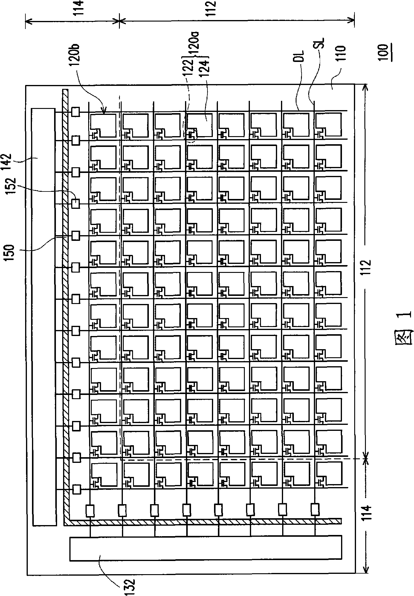
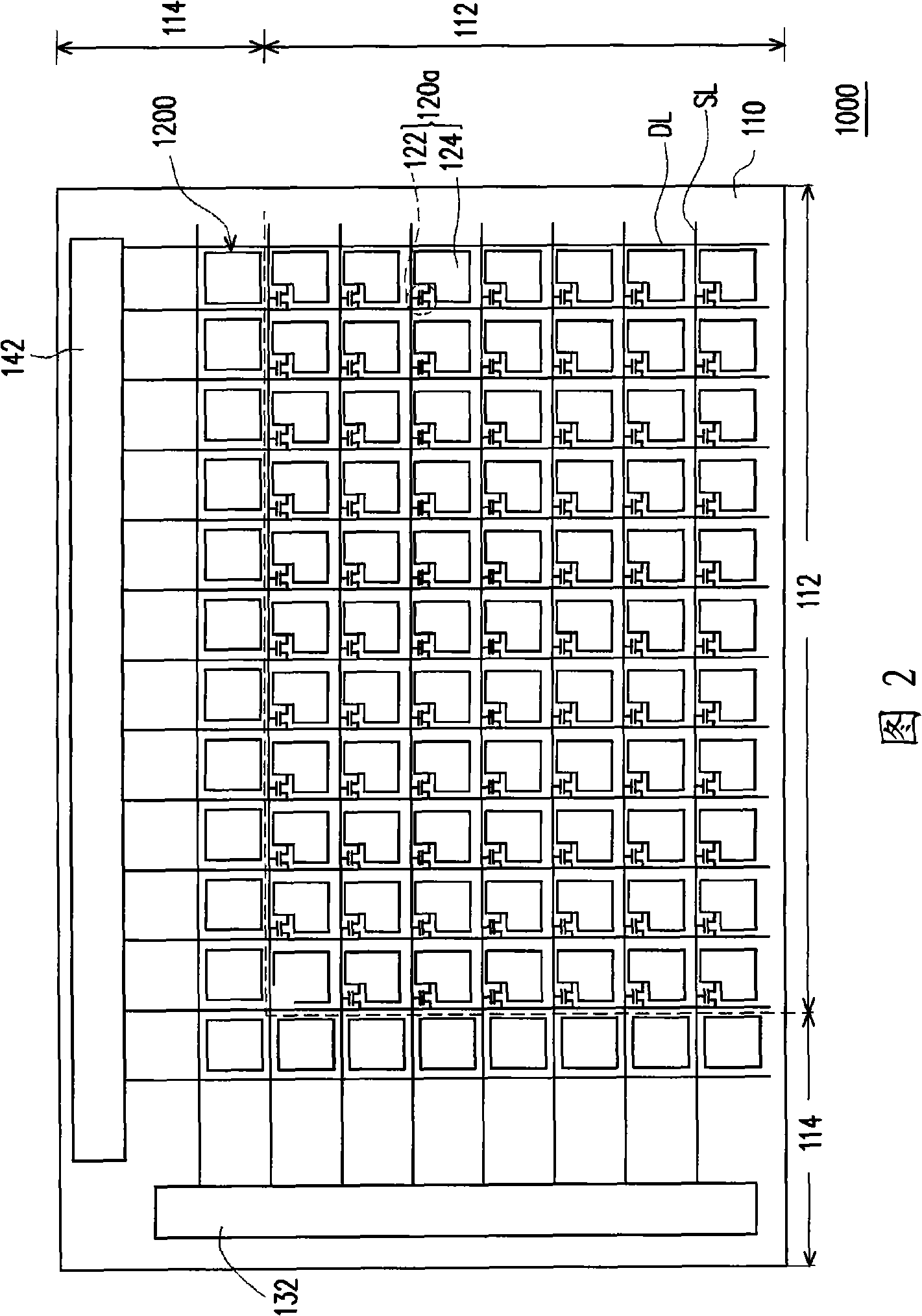
[0068] figure 2 It is a schematic diagram of the pixel array substrate according to the first embodiment of the present invention. Please refer to figure 2 The pixel array substrate 1000 includes a substrate 110 , a plurality of scan lines SL and data lines DL, a plurality of pixel units 120 a and a plurality of pseudo pixel units 1200 . The substrate 110 has a pixel area 112 and a wiring area 114 adjacent to the pixel area 112 . The scanning lines SL and the data lines DL are arranged in the pixel area 112 of the substrate 110, and one end of each scanning line SL and one end of each data line DL will extend into the wiring area 114, and connect with the gate driving circuit area 132 and the source The components of the pole driving circuit area 142 are electrically connected. Each pixel unit 120 a is composed of a thin film transistor 122 and a pixel electrode 124 , and each pixel unit is electrically connected to the corresponding scan line SL and data line DL.

[006...

no. 2 example

[0084] This embodiment is substantially the same as the first embodiment, and the same or similar component numbers represent the same or similar components. Wherein, the configurations of the display pixel unit and the dummy pixel unit 2200 of the pixel array substrate in this embodiment are substantially the same, so details are not repeated here.

[0085] Figure 5A is a schematic diagram of a single quasi-pixel unit of the pixel array substrate in the second embodiment of the present invention, and Figure 5B for Figure 5A Schematic diagram of the equivalent circuit of the quasi-pixel unit. Please also refer to Figure 5A and 5B Each pseudo pixel unit 2200 in this embodiment includes a data line DL, a scan line SL, a first switch component 2230, a second switch component 2240, a first pixel electrode 2280, a third switch component 2250, A fourth switch element 2260, a second pixel electrode 2290 and a sharing line CL.

[0086] In this embodiment, the sharing line CL...

no. 3 example

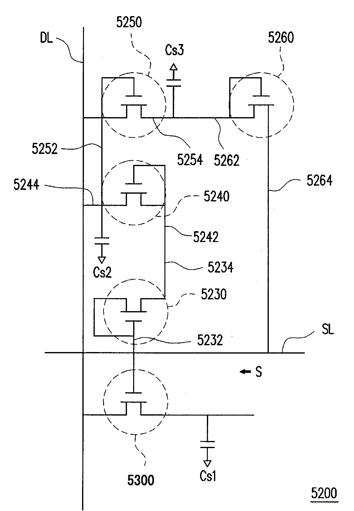
[0092] This embodiment is substantially the same as the second embodiment, and the same or similar component numbers represent the same or similar components. The similarities will not be repeated.

[0093] Figure 6 It is a schematic diagram of an equivalent circuit of a single quasi-pixel unit of the pixel array substrate according to the third embodiment of the present invention. Please refer to Figure 6 The difference between this embodiment and the second embodiment lies in that: one end 3232 of the first switch component 3230 is connected to the scan line SL.

[0094] After the static electricity S is transmitted from the scan line SL, the static electricity S will be transferred from the first switch component 3230 and the second switch component 2240 to the sharing line CL and dissipated. In addition, the static electricity S can also be transferred to the data line DL by the fourth switch component 2260 and the third switch component 2250 and dissipated.

[0095]...


PUM


Abstract

The invention provides a pixel array substrate which is provided with a pixel area and a wiring area which is positioned at the edge of the pixel area. The pixel array substrate comprises a plurality of display pixel units in the pixel area and a plurality of imitation-pixel units in the wiring area; wherein, each imitation-pixel unit comprises a data line and a scanning line, a plurality of switch components and a plurality of pixel electrodes. The switch component is electrically connected with the data line and the scanning line; and the pixel electrode is electrically connected with the switch component. More especially, the electrostatic current in the pixel area can be dispersed by the imitation-pixel unit in the wiring area. The imitation-pixel unit can maintain the electric continuity of the pixel array substrate and provides the protection effect of the electrostatic discharging simultaneously. Therefore, the wiring area of the pixel array substrate has large area.

Description

【Technical field】 [0001] The present invention relates to a pixel array substrate, and in particular to a pixel array substrate with a large wiring area. 【Background technique】 [0002] In recent years, due to the maturity of optoelectronic technology and semiconductor manufacturing technology, the vigorous development of flat-panel displays has been driven. Among them, liquid crystal displays have become the mainstream of display products due to their advantages of low-voltage operation, no radiation scattering, light weight, and small size. [0003] A general liquid crystal display is mainly assembled by a liquid crystal display panel and a backlight module. Among them, the liquid crystal display panel is generally composed of a pixel array substrate including a thin film transistor array, a color filter substrate, and a liquid crystal layer between the two, wherein many scanning lines, data Very fine lines and components such as lines and pixel units. [0004] figure 1...

Claims


Application Information

Patent Timeline
Patent Type & Authority Patents(China)
IPC IPC(8): G02F1/1362
Inventor 康良豪张营辉
Owner CPT TECH GRP
Why Eureka
Try Eureka