Erasing and writing method for FLASH memory
A FLASH memory, data frame technology, applied in the protection of storage content to prevent loss, memory address/allocation/relocation, etc., can solve the problems of high cost, complex circuit design, occupied space, etc., to achieve high speed and save PCB. space and cost saving
- Summary
- Abstract
- Description
- Claims
- Application Information
AI Technical Summary
Problems solved by technology
Method used
Image
Examples
Embodiment Construction
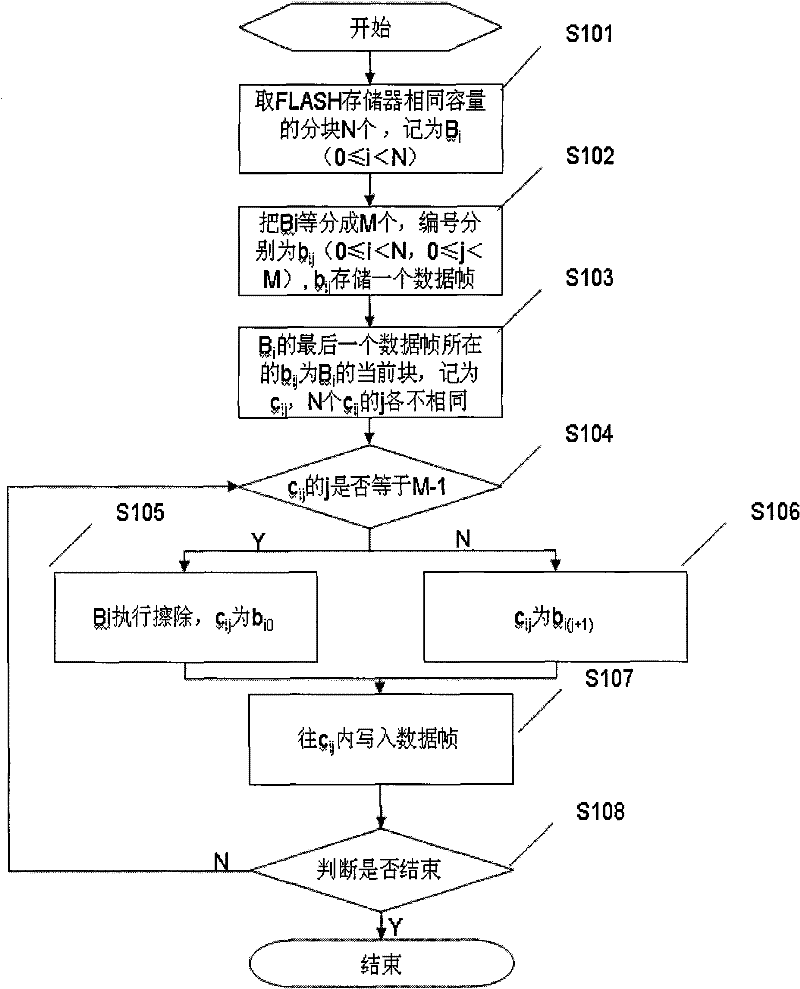
[0028] Such as figure 1 Shown, in the erasing and writing method of FLASH memory of the present invention, this method comprises the following steps:
[0029] S101. Take N blocks of the same capacity of the FLASH memory, denoted as B i (0≤ii (0≤i
[0030] S102. Put B i Divide into M pieces equally, numbered b ij (0≤iij For storing a data frame, the data frame includes 8 times the number of bytes;
[0031] S103.B i where the last data frame of b ij for B i The current block of , denoted as c ij , N c ij j varies;
[0032] S104. Judging c ij Whether j is equal to M-1, if so, go to step S105; otherwise go to step S106;
[0033] S105.B i perform erase, c ij for b i0 , and then turn to step S107;
[0034] S106.c ij for b i(j+1) ;
[0035] S107. to c ij Write data frame inside;
[0036] S108. Determine whether to end, if yes, end the operation of the FLASH memory; if not, then go to step S104.
[0037] Figure 2A to Figur...
PUM
 Abstract
Description
Claims
Application Information


