

Semiconductor wafer and pattern alignment method
A semiconductor and wafer technology, applied in the field of pattern alignment methods and design structures for manufacturing these semiconductor components, can solve problems such as unsatisfactory alignment of alignment technology, and achieve the effect of improving alignment
- Summary
- Abstract
- Description
- Claims
- Application Information
AI Technical Summary
Problems solved by technology
Method used
Image

Examples
Embodiment Construction
[0038] It can be appreciated that the following disclosure provides many different embodiments, or examples, for implementing different features of the invention. Specific examples of components and arrangements are described below to simplify the present invention. Of course these are examples only, not limitations. In addition, the present invention may repeat reference numerals and / or characters in each example. Such repetition is for simplicity and clarity and is not, by itself, intended to dictate a relationship between the various embodiments and / or configurations discussed. Furthermore, in the description, a first feature formed on or over a second feature may include embodiments in which the first and second features are formed in direct contact, and may also include that additional features may be formed on the first and second features. Embodiments between two features such that the first and second features may not be in direct contact.
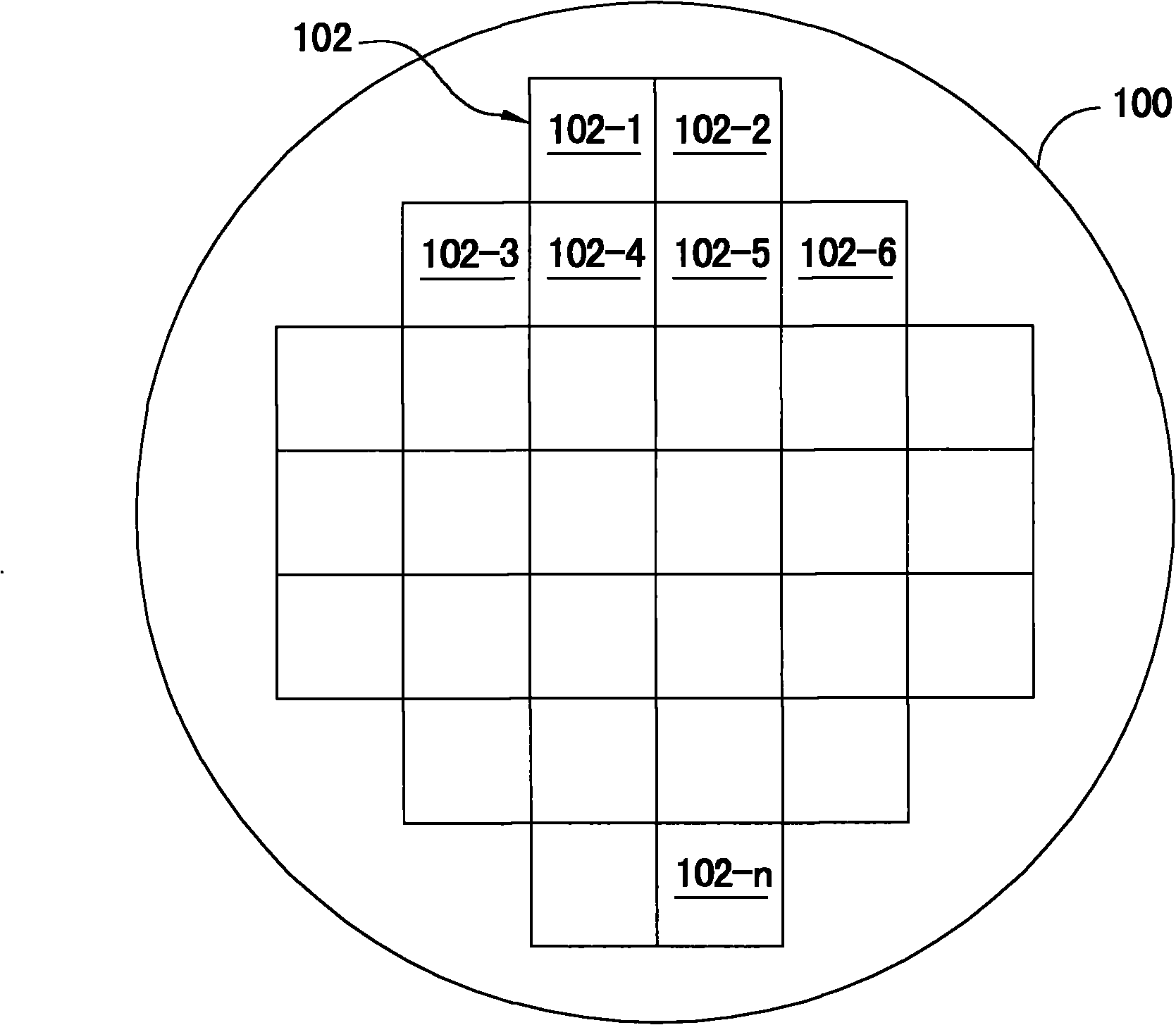
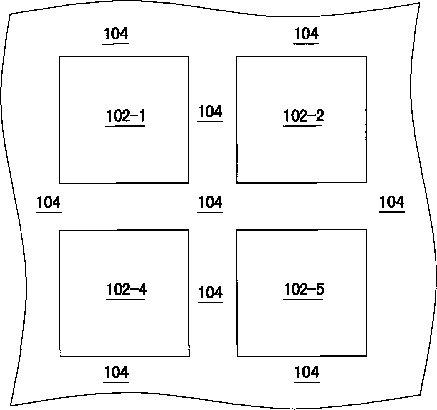
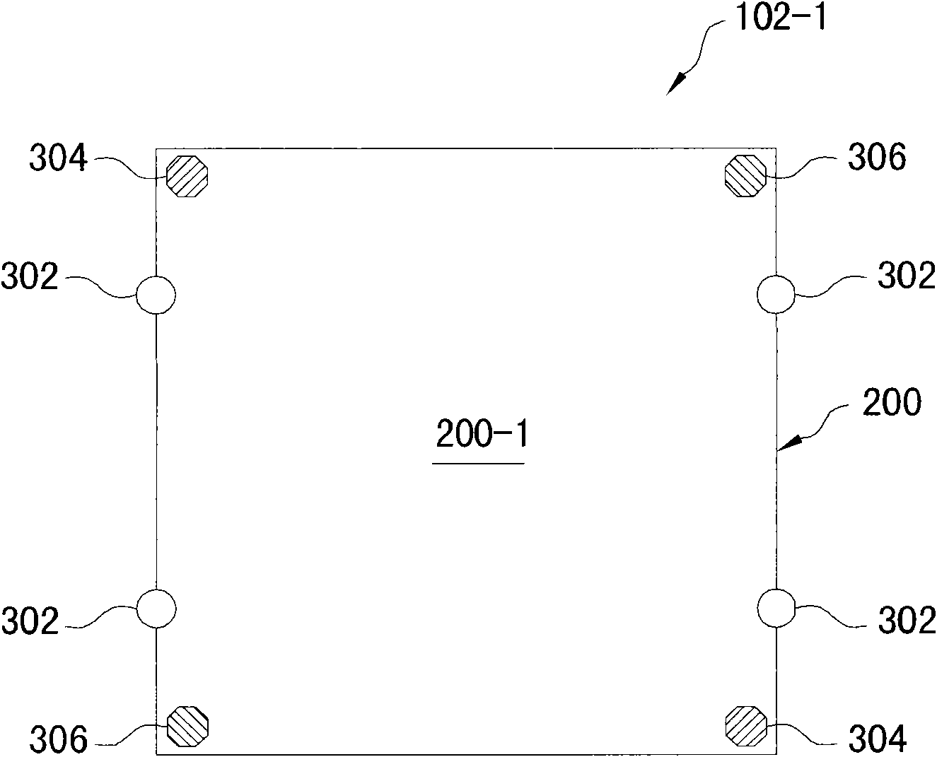
[0039] figure 1 A wafer...
PUM
 Abstract
Description
Claims
Application Information