Method for detecting interlayer offset and drilling offset of multi-layer circuit board

A technology of offset detection and multi-layer circuit, which is applied in the direction of measuring devices and instruments, can solve the problems of inability to judge the offset of drilling holes and the inability to directly read the offset between layers, so as to save production time and reduce the risk of scrapping , the effect of easy operation

Active Publication Date: 2012-05-23
VICTORY GIANT TECH HUIZHOU CO LTD
View PDF1 Cites 0 Cited by
  • Summary
  • Abstract
  • Description
  • Claims
  • Application Information

AI Technical Summary

Problems solved by technology

This method solves the technical problems of the longitudinal slicing method, but it also has many defects. It can only judge the offset of the CORE by setting the etched ring on the odd or even layer, but it cannot judge the offset of the drill hole. , it is not possible to directly judge the offset of a specific layer, and it is not possible to directly read the interlayer offset by measuring the resistance meter

Method used


Image

  • Method for detecting interlayer offset and drilling offset of multi-layer circuit board
  • Method for detecting interlayer offset and drilling offset of multi-layer circuit board

Examples


Embodiment Construction

[0015] In order to facilitate the understanding of those skilled in the art, the present invention will be further described in detail below in conjunction with the embodiments.

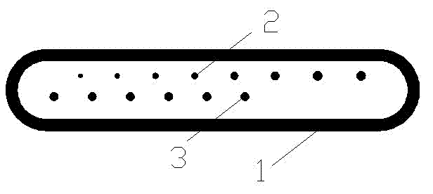
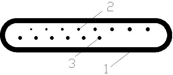
[0016] This embodiment adopts the technical solution of the present invention to realize accurate detection of interlayer and drilling offset of eight-layer circuit boards, including the following steps: The detection module is set at the corner of the board, such as figure 1 As shown, the detection module includes an isolation frame composed of two parallel copper strips and copper semi-circular rings connected at both ends of the two parallel copper strips. Measurement ring 2 and monitoring ring 3 for several level offsets.

[0017] The above-mentioned isolation frame is used to isolate the detection pattern to prevent the connection with other graphics from destroying the integrity of other graphics. The length of the two parallel copper strips of the isolation frame is 23.5MM and the width is 3....


PUM


Abstract

The present invention relates to a method for detecting an interlayer offset and a drilling offset of a multi-layer circuit board, which comprises arranging detection modules in the middle of each long edge and at board corners of each short edge outside a formation area of each layer of circuit board. The detection modules comprise an isolating frame, a plurality of hole offset measuring rings and a plurality of layer offset monitoring rings, wherein the isolating frame comprises two parallel copper bars and copper semicircular rings connected with the two ends of the two parallel copper bars, the hole offset measuring rings and the layer offset monitoring rings are arranged on the copper bars of the isolating frame with the same spacing, the centers of the hole offset measuring rings and the layer offset monitoring rings are arranged linearly, the hole offset measuring rings comprise 6-8 copper-free rings, the parts of each layer of circuit board for the copper-free rings are removed, the spacing of the copper-free rings on each layer of circuit board is 1.98MM, and the midpoint of the straight line for arrangement of the centers of the copper-free rings is 0.9MM away from the outer edges of the copper bars of the isolating frame and 6MM away from the ends of the copper semicircular rings. Since the detection modules are arranged in the middle of each long edge and at the board corners of each short edge outside the formation area of each layer of circuit board, the offset of all internal layers of the multi-layer circuit board can be detected comprehensively, the interlayer offset and the drilling offset can be detected simultaneously, and the offset can be read directly.

Description

technical field [0001] The invention relates to the technical field of multilayer circuit board production, in particular to a detection method for interlayer and drilling offset of a multilayer circuit board. Background technique [0002] Circuit boards are divided into single-sided, double-sided and multi-layer circuit boards according to the number of layers. Due to the increase in the packaging density of integrated circuits, the interconnection lines are highly concentrated, which makes multi-layer circuit boards gradually widely used. Each layer of a multilayer circuit board is composed of upper and lower inner layers of copper foil and an insulating layer between them, and each layer is bonded to each other by an adhesive, and the copper foils of each layer are not connected. state. Therefore, in order to realize the interconnection between the circuits of each layer, it is necessary to form a through hole by drilling, and then electroplate the through hole to form a...

Claims


Application Information

Patent Timeline
Patent Type & Authority Patents(China)
IPC IPC(8): G01B21/02
Inventor 李加余龚俊
Owner VICTORY GIANT TECH HUIZHOU CO LTD
Why Eureka
Try Eureka