Integrated circuit structure and formation method thereof

An integrated circuit, gate dielectric technology, applied in circuits, electrical components, semiconductor devices, etc., to reduce the current crowding effect, increase tension and compressive stress

Active Publication Date: 2013-06-12
TAIWAN SEMICON MFG CO LTD
View PDF4 Cites 0 Cited by
  • Summary
  • Abstract
  • Description
  • Claims
  • Application Information

AI Technical Summary

Problems solved by technology

The first fin height is greater than the second fin height

Method used


Image

  • Integrated circuit structure and formation method thereof
  • Integrated circuit structure and formation method thereof
  • Integrated circuit structure and formation method thereof

Examples


Embodiment Construction

[0032] Several different embodiments are provided due to different features of the invention. The specific elements and arrangements in the present invention are for simplicity, but the present invention is not limited to these embodiments. For example, a description of forming a first element on a second element may include embodiments in which the first element is in direct contact with the second element, as well as embodiments having additional elements formed between the first element and the second element such that the second element An embodiment in which one element is not in direct contact with a second element.

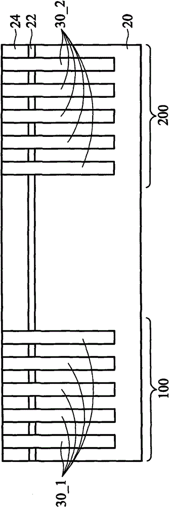
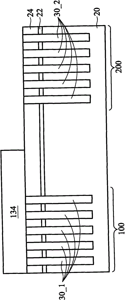
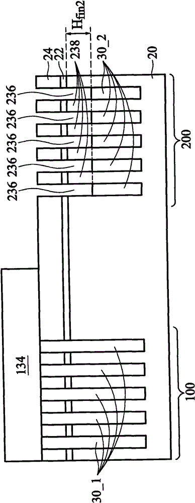
[0033] The present invention provides a novel method to form semiconductor fins and FinFETs with different fin heights. This disclosure illustrates intermediate steps in the manufacture of embodiments and discusses various embodiments. In the illustrations and descriptions of the respective embodiments, similar elements are denoted by similar reference nu...


PUM


Abstract

The invention provides an integrated circuit structure and a formation method thereof, and the structure comprises a first portion in which a semiconductor substrate is contained in a first element region, and a second portion in which a semiconductor substrate is contained in a second element region. A first semiconductor fin is over the semiconductor substrate and has a first fin height. A second semiconductor fin is over the semiconductor substrate and has a second fin height. The first fin height is greater than the second fin height. The invention has a positive effect on the reduction of the current crowding at the source electrode and the drain electrode regions. Because of the volume increase of the stress source electrode and the drain electrode regions, the tension and the compression strain on the channel region of a fin-type field effect transistor are increased.

Description

technical field [0001] The present invention relates to integrated circuits, and in particular to a semiconductor fin plate, a fin field-effect transistor (Fin field-effect transistor; FinFet) and a forming method thereof. Background technique [0002] With the continuous down-scaling of integrated circuits and the increase of high-speed requirements for integrated circuits, transistors must have higher driving currents while the size is continuously reduced. In order to meet the above requirements, FinFETs have been developed. Since the channel of the FinFET has an extra sidewall portion besides the top surface of the fin plate, the channel width increases. Since the driving current of the transistor is proportional to the channel width, the driving current of the FinFET is larger than that of the planar transistor. Contents of the invention [0003] In order to overcome the above disadvantages of the prior art, according to an embodiment of the present invention, the i...

Claims


Application Information

Patent Timeline
Patent Type & Authority Patents(China)
IPC IPC(8): H01L29/78H01L21/336H01L21/8234
Inventor 李宗霖叶致锴张长昀袁锋
Owner TAIWAN SEMICON MFG CO LTD
Why Eureka
Try Eureka