Improved power semiconductor device and preparation method thereof

An improved technology for power semiconductors, applied in semiconductor devices, electrical components, circuits, etc., can solve the problems of high device turn-on voltage, high production cost, complex process, etc., and achieve the effect of avoiding device damage and improving latch-up resistance

Inactive Publication Date: 2017-05-31
CR TECH PINGTAN CO LTD
View PDF2 Cites 0 Cited by
  • Summary
  • Abstract
  • Description
  • Claims
  • Application Information

AI Technical Summary

Problems solved by technology

[0006] The purpose of the present invention is to provide an improved power semiconductor device and its preparation method, aiming to solve the problem that existing methods for improving latch-up resistance may increase gate and source short-circuit failure rates, or make the device turn-on voltage high and parameters unstable At the same time, there are problems of complex process and high production cost

Method used


Image

  • Improved power semiconductor device and preparation method thereof
  • Improved power semiconductor device and preparation method thereof
  • Improved power semiconductor device and preparation method thereof

Examples


Embodiment Construction

[0014] In order to make the object, technical solution and advantages of the present invention more clear, the present invention will be further described in detail below in conjunction with the accompanying drawings and embodiments. It should be understood that the specific embodiments described here are only used to explain the present invention, not to limit the present invention.

[0015] In the description of the present invention, it should be understood that the terms "first" and "second" are used for description purposes only, and cannot be interpreted as indicating or implying relative importance or implicitly indicating the quantity of indicated technical features. Thus, a feature defined as "first" and "second" may explicitly or implicitly include one or more of these features.

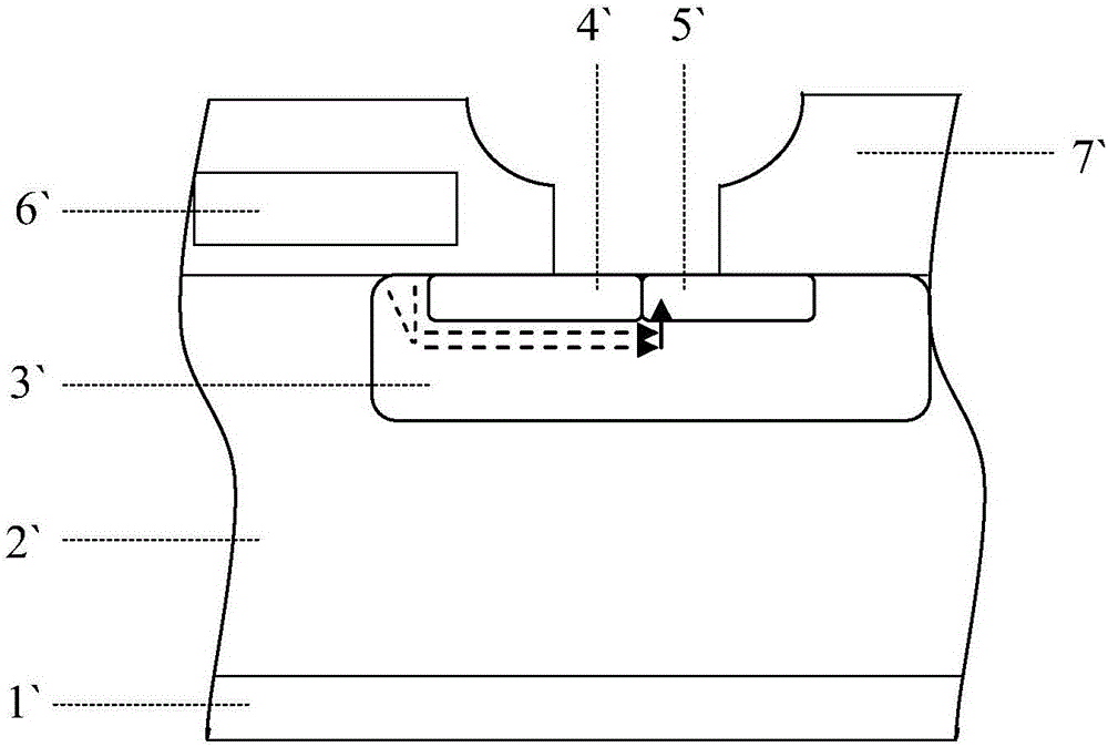
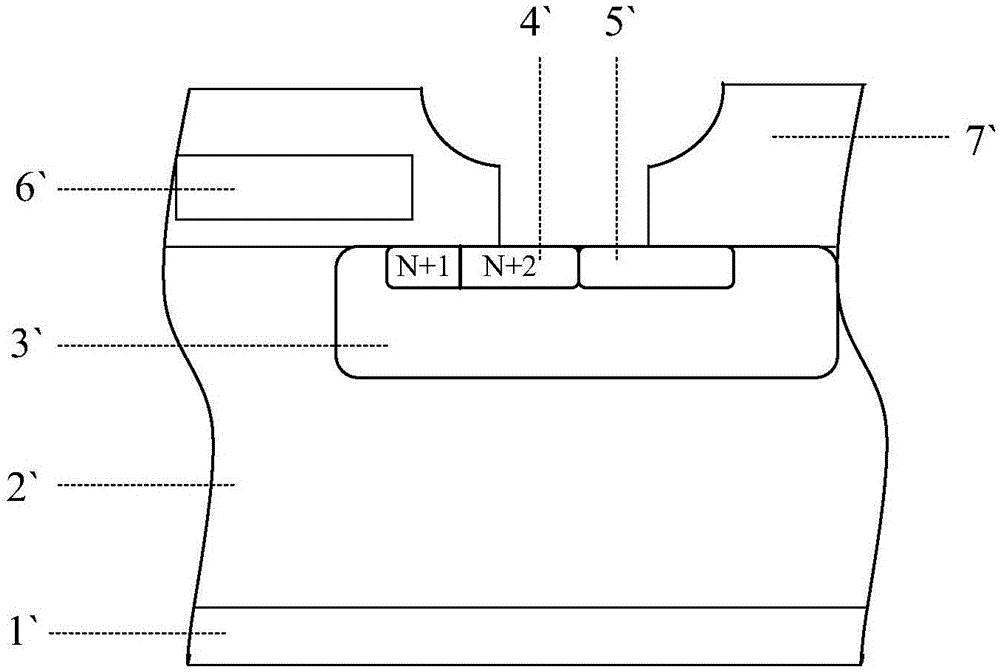
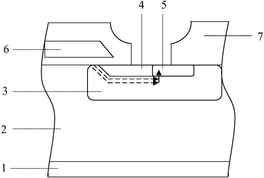
[0016] Such as image 3 As shown, one embodiment of the present invention provides an improved power semiconductor device, including a plurality of cellular MOS devices, the polycrystallin...


PUM


Abstract

The invention belongs to the technical field of semiconductor power devices and provides an improved power semiconductor device and a preparation method thereof. The improved power semiconductor device comprises a plurality of cell MOS (Metal Oxide Semiconductor) devices, a polycrystalline grid of each cell MOS device has an inclined side wall, and a source region of each cell MOS device has gradient type concentration distribution; the distance between an upper angle of each polycrystalline grid and metal of the source region is enlarged through the inclination of a side wall of the polycrystalline grid, the failure rate of grid and source short circuits is reduced, the transverse resistance of a well region under the polycrystalline grid is reduced, and the latch-proof capability of the device is improved; and meanwhile, the gradient type concentration distribution is formed by injecting an element into the source region for one time, so that the process is simplified, the phenomenon that current crowding is formed between the source region of hole current and a corner of a depletion region of the well region is reduced, and conditions that the current is concentrated and the device is damaged are avoided.

Description

technical field [0001] The invention belongs to the technical field of semiconductor power devices, and in particular relates to an improved power semiconductor device and a preparation method thereof. Background technique [0002] In the field of electronic technology, power semiconductor devices are key components, and their characteristics play a vital role in the realization and improvement of system performance. Currently used power devices are mainly MOSFET (Metal-Oxide-Semiconductor Field-Effect Transistor, Metal-Oxide Semiconductor Field Effect Transistor) and IGBT (Insulated Gate Bipolar Transistor, insulated gate bipolar transistor). Among them, IGBT is the natural evolution of vertical power MOSFET for high current, high voltage application and fast terminal equipment. [0003] Both MOSFET and IGBT are controlled by the gate voltage. When the gate voltage exceeds the rated turn-on voltage, the device remains in the on state; due to the P-N-P-N four-layer structur...

Claims


Application Information

Patent Timeline
Patent Type & Authority Applications(China)
IPC IPC(8): H01L33/20H01L33/38H01L33/00
CPCH01L33/38H01L33/005H01L33/20
Inventor 黄国华蔡荣怀陈孟邦曹进伟乔世成
Owner CR TECH PINGTAN CO LTD
Why Eureka
Try Eureka