LED epitaxial wafer, manufacturing method thereof, and LED chip including same

A technology of LED epitaxial wafers and manufacturing methods, which is applied to electrical components, circuits, semiconductor devices, etc., can solve the problems of high driving voltage and low brightness, and achieve the effects of reducing light absorption, increasing light-emitting area, and improving brightness and light efficiency

Active Publication Date: 2016-06-29
XIANGNENG HUALEI OPTOELECTRONICS
View PDF3 Cites 0 Cited by
  • Summary
  • Abstract
  • Description
  • Claims
  • Application Information

AI Technical Summary

Problems solved by technology

[0006] The present invention aims to provide an LED epitaxial wafer, a manufacturing method thereof and an LED chip including the same, so as to solve the technical problems of high driving voltage and low brightness existing in existing high-power LED devices

Method used


Image

  • LED epitaxial wafer, manufacturing method thereof, and LED chip including same
  • LED epitaxial wafer, manufacturing method thereof, and LED chip including same
  • LED epitaxial wafer, manufacturing method thereof, and LED chip including same

Examples


Embodiment 1

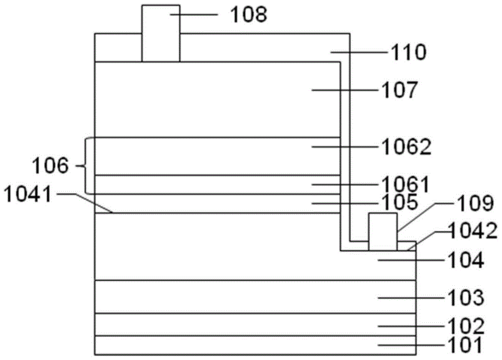
[0061] This embodiment provides a method for manufacturing an LED chip. The method includes forming an epitaxial layer on the surface of a substrate, forming a tunnel junction layer on the epitaxial layer, and manufacturing a P electrode, an N electrode, and a protective layer.

[0062] Step S1, forming an epitaxial layer on the surface of the substrate, comprising the following steps:

[0063] Raise the temperature from room temperature to 1100°C in 490 seconds, and process the sapphire substrate for 5 minutes under the conditions of hydrogen atmosphere and reaction chamber pressure of 180mbar;

[0064] Cool down to 560°C in 420 seconds, control the pressure of the reaction chamber at 480mbar, and grow a GaN buffer layer with a thickness of 40nm on the sapphire substrate;

[0065] After 350 seconds, the temperature was raised to 1100°C, the pressure of the reaction chamber was controlled at 480mbar, and the undoped GaN of 2.5μm was continuously grown, that is, the first U-typ...

Embodiment 2

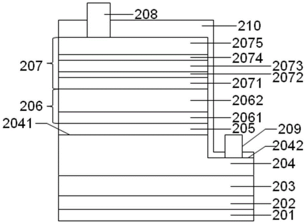
[0078] This embodiment provides a method for manufacturing an LED chip. The method includes forming an epitaxial layer on the surface of a substrate, forming a tunnel junction layer on the epitaxial layer, and manufacturing a P electrode, an N electrode, and a protective layer.

[0079] In this embodiment, the step of forming an epitaxial layer on the surface of the substrate is the same as the step S1 of the first embodiment, and the steps of forming the N electrode, the P electrode and the protective layer are the same as the step S3 of the first embodiment.

[0080] The step of forming a tunnel junction layer on the epitaxial layer is different from step S2 in embodiment 1. In this embodiment, step S2 is:

[0081] Keep the temperature at 1000°C, the pressure in the reaction chamber at 200mbar, control the flow rate of Mg to 2500sccm, and grow a heavily doped P-type GaN layer with a thickness of 20nm, that is, the second P-type GaN layer, in which the doping concentration of ...

Embodiment 3

[0085] This embodiment provides a method for manufacturing an LED chip. The method includes forming an epitaxial layer on the surface of a substrate, forming a tunnel junction layer on the epitaxial layer, and manufacturing a P electrode, an N electrode, and a protective layer.

[0086] In this embodiment, the step of forming an epitaxial layer on the surface of the substrate is the same as the step S1 of the first embodiment, and the steps of forming the N electrode, the P electrode and the protective layer are the same as the step S3 of the first embodiment.

[0087] The step of forming a tunnel junction layer on the epitaxial layer is different from step S2 in embodiment 1. In this embodiment, step S2 is:

[0088] Keep the temperature at 1100°C, the pressure in the reaction chamber at 600mbar, control the flow of Mg to 2600sccm, and grow a heavily doped P-type GaN layer with a thickness of 30nm, that is, the second P-type GaN layer, in which the doping concentration of Mg is...


PUM


Abstract

The invention discloses an LED epitaxial wafer, a manufacturing method of the LED epitaxial wafer and an LED chip with the LED epitaxial wafer. The LED epitaxial wafer comprises a GaN buffer layer, a first U type GaN layer, a first N type GaN layer, a quantum well layer and a first P type GaN layer, wherein the GaN buffer layer, the first U type GaN layer, the first N type GaN layer, the quantum well layer and the first P type GaN layer are sequentially and outward arranged from the surface of a substrate. The LED epitaxial wafer further comprises a tunnel junction layer arranged on the first P type GaN layer. The manufacturing method of the LED epitaxial wafer includes the following steps of sequentially and outward forming the GaN buffer layer, the first U type GaN layer, the first N type GaN layer, the quantum well layer and the first P type GaN layer from the surface of the substrate, and forming the tunnel junction layer on the first P type GaN layer. The driving voltage of an LED obtained through the manufacturing method of the LED epitaxial wafer is lowered, and the luminance and the luminous efficiency are improved.

Description

technical field [0001] The invention relates to the technical field of semiconductor lighting, in particular to an LED epitaxial wafer, a manufacturing method thereof and an LED chip comprising the same. Background technique [0002] GaN-based materials (including GaN, AlGaN, InGaN, MgGaN, and SiGaN) are direct bandgap semiconductors, and their bandgap is continuously adjustable from 1.8-6.2V. They are the most commonly used materials for producing high-brightness blue, green, and white LEDs. It is widely used in fields such as backlight, large-size screen display, signage indication, signal lamp and lighting. [0003] The manufacturing method of GaN-based LED chips is usually: using MOCVD (metal organic compound chemical vapor deposition method) to epitaxially grow a layer of GaN buffer layer on the sapphire substrate; On this basis, N-type GaN doped with Si, GaN quantum wells doped with In, and P-type GaN doped with Mg or Al are grown sequentially to form LED epitaxial wa...

Claims


Application Information

Patent Timeline
Patent Type & Authority Patents(China)
IPC IPC(8): H01L33/04H01L33/00
Inventor 张宇
Owner XIANGNENG HUALEI OPTOELECTRONICS
Why Eureka
Try Eureka