

Method and system for an improved power distribution network for use with a semiconductor device
a technology for power distribution networks and semiconductor devices, applied in semiconductor devices, semiconductor/solid-state device details, electrical apparatus, etc., can solve problems such as reducing the impedance of pcb, and achieve the effects of reducing current crowding, increasing the impedance of the package or reducing the impedance of the pcb, and increasing the impedance of the packag
- Summary
- Abstract
- Description
- Claims
- Application Information
AI Technical Summary
Benefits of technology
Problems solved by technology
Method used
Image

Examples
Embodiment Construction
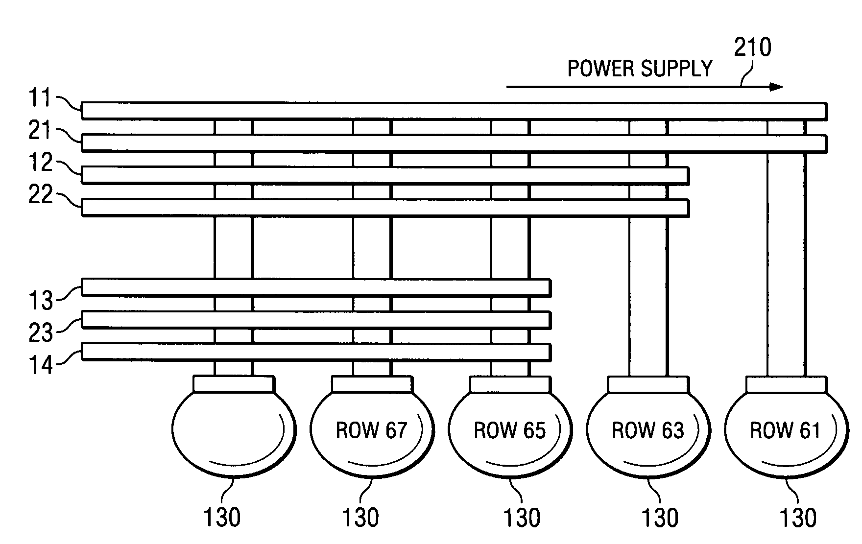
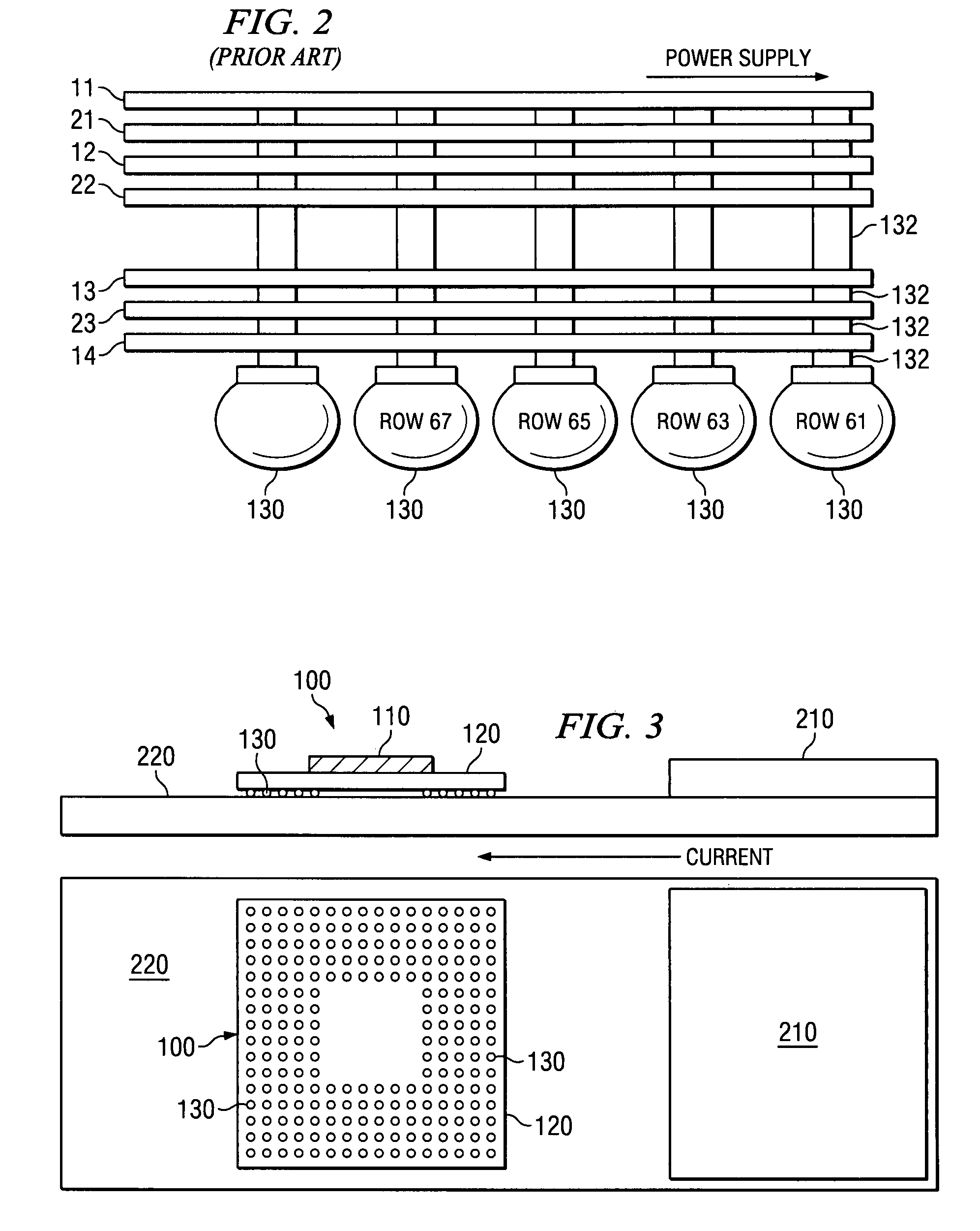
[0040]The invention and the various features and advantageous details thereof are explained more fully with reference to the nonlimiting embodiments that are illustrated in the accompanying drawings and detailed in the following description. Descriptions of well known starting materials, processing techniques, components and equipment are omitted so as not to unnecessarily obscure the invention in detail. Skilled artisans should understand, however, that the detailed description and the specific examples, while disclosing preferred embodiments of the invention, are given by way of illustration only and not by way of limitation. Various substitutions, modifications, additions or rearrangements within the scope of the underlying inventive concept(s) will become apparent to those skilled in the art after reading this disclosure.
[0041]Reference is now made in detail to the exemplary embodiments of the invention, examples of which are illustrated in the accompanying drawings. Wherever po...
PUM
 Abstract
Description
Claims
Application Information