LED (Light-Emitting Diode) plane light source and method for increasing light guiding efficiency thereof

A technology of LED light source and plane light source, applied in the field of light sensing engineering application, can solve the problems of affecting the brightness of lamps, reducing the luminous efficiency of lamps, light loss, etc., and achieving the effects of reducing light absorption, saving costs, and reducing the number of use

Inactive Publication Date: 2011-06-01
PUHUAN OPTOELECTRONICS TECH SHANGHAI
View PDF0 Cites 4 Cited by
  • Summary
  • Abstract
  • Description
  • Claims
  • Application Information

AI Technical Summary

Problems solved by technology

Existing LED planar light sources have light distribution on one side of the light guide plate, and there are also secondary light distribution methods, that is, LED light sources are installed on opposite sides of the light guide plate, but when the light emitted by the LED reaches the side of the light guide plate, it will produce total reflection. A part of the incident light is lost, and when it reaches the opposite side through the light guide plate, part of the light can be absorbed by the opposite LED and the PCB circuit board on which the LED is fixed. Similarly, the opposite LED passes through the light guide plate and irradiates the LED and PCB on this side. On the circuit board, it will also lead to further loss of light, which will reduce the luminous efficiency of the overall lamp and affect the brightness of the lamp

Method used


Image

  • LED (Light-Emitting Diode) plane light source and method for increasing light guiding efficiency thereof
  • LED (Light-Emitting Diode) plane light source and method for increasing light guiding efficiency thereof
  • LED (Light-Emitting Diode) plane light source and method for increasing light guiding efficiency thereof

Examples


Embodiment Construction

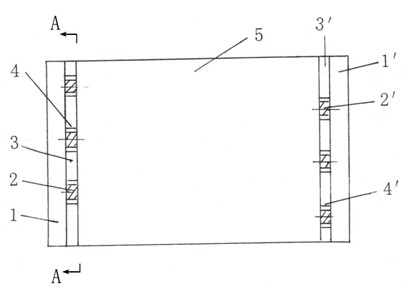
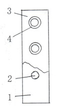
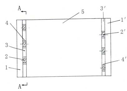
[0014] Depend on figure 1 and figure 2 As shown in the figure, a flat LED light source includes a light guide plate 5, LED light sources 2 respectively placed on opposite sides of the light guide plate 5, and a PCB circuit board 1 for fixing the LED light source 2 by welding. A layer of reflective layer 3 is placed between the side of the light plate 5 and the PCB circuit board 1, and a light outlet 4 is preset on the reflective layer 3 at the corresponding position of the LED light source 2, and the PCB circuit board 1-reflective layer 3 - The light guide plates 5 are closely attached to each other in sequence; the LED light sources 2 respectively placed on the opposite sides of the light guide plate 5 are intersected with each other and arranged complementary to each other.

[0015] The LED light source 2 is an LED lamp bead.

[0016] The reflective layer 3 is a PET light reflective film.

[0017] The method for improving the light-guiding efficiency of the LED flat ligh...


PUM


Abstract

The invention relates to an LED (Light-Emitting Diode) plane light source and a method for increasing the light guiding efficiency thereof, belonging to the technical field of light sensing engineering application. The LED plane light source is characterized in that a light reflection layer is arranged between the side of a light guiding plate and a PCB (Printed Circuit Board), a light outlet is prearranged at a position on the light reflection layer corresponding to LED light sources, and the PCB, the light reflection layer and the light guiding plate clings to each other in sequence; and the LED light sources respectively arranged at two opposite sides of the light guiding plate are arranged in ways of mutual cross and ectopic complementation. One side of each of the LED light sources is additionally provided with the light reflection layer on which the light outlet is prearranged, thus the light reflection at the side of the light guiding plate is avoided, light emitted by an LED is directly led out through the light outlet by the light guiding plate, and the light incidence efficiency is increased; the LED light sources are arranged in ways of mutual cross and ectopic complementation, thus, the condition that the LED absorbs the light from the opposite LED per se is avoided, and the light guiding efficiency is increased; and on the basis of ensuring same brightness, the consumption of the LEDs can be reduced and the lost can be lowered.

Description

technical field [0001] The invention belongs to the technical field of light sensing engineering application, and relates to an LED plane light source and a method for improving light guiding efficiency. Background technique [0002] LED is a semiconductor light-emitting diode that converts electrical energy into visible light. Because LED has the advantages of high light efficiency, long service life, no radiation and low power consumption, it is an environmentally friendly green lighting source, so various LEDs Lamps have developed rapidly and have been widely used in daily life. In the field of development and application of flat lights, it has also attracted widespread attention. There are many manufacturers engaged in the research and development and production of LED flat lights and LED ultra-thin light boxes. [0003] LED flat light source is mainly composed of LED light source, light guide plate and frame, etc. It has the advantages of small size, thin thickness, no...

Claims


Application Information

Patent Timeline
Patent Type & Authority Applications(China)
IPC IPC(8): F21S2/00F21V7/22F21V19/00F21Y101/02F21K9/20F21Y115/10
Inventor 陈冬生崔黎明吴斌王鑫
Owner PUHUAN OPTOELECTRONICS TECH SHANGHAI
Why Eureka
Try Eureka