
Integrated circuit structure

An integrated circuit and substrate technology, applied in the field of fin field effect transistors, can solve the problems of increasing effective source/drain resistance, increasing current congestion, etc., and achieve the effect of increasing distance and reducing current congestion

Active Publication Date: 2013-06-12
TAIWAN SEMICON MFG CO LTD
View PDF0 Cites 0 Cited by
  • Summary
  • Abstract
  • Description
  • Claims
  • Application Information

AI Technical Summary

Problems solved by technology

The above profile will seriously lead to an increase in current crowding
Additionally, the effective source / drain resistance increases

Method used


Image

  • Integrated circuit structure
  • Integrated circuit structure
  • Integrated circuit structure

Examples


Embodiment Construction

[0048] The present invention provides a novel fin field-effect transistor (FinFET) and its forming method, and discusses the differences of various embodiments. In all the different views and illustrated embodiments, the same reference numerals are used to designate the same elements.

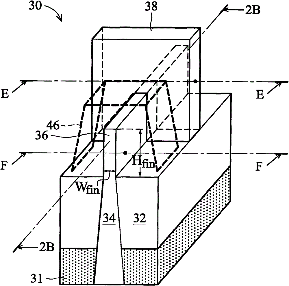
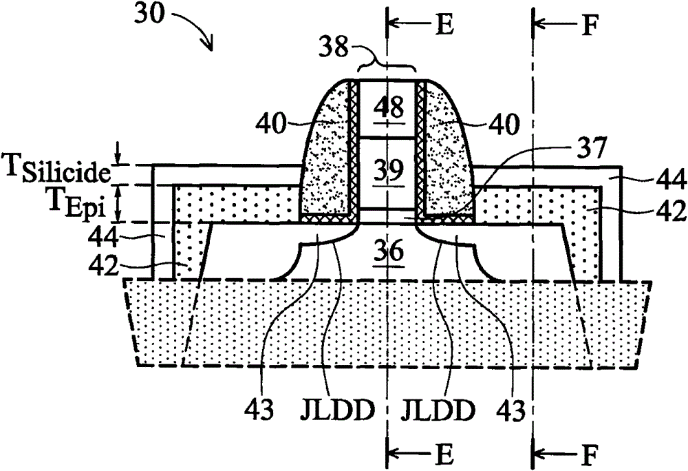
[0049] Figure 2A A perspective view of a fin field effect transistor (FinFET) 30 including a fin 36 and a gate stack 38 on the upper surface and sidewalls of the fin 36 is disclosed. For simplicity, the gate spacer 40, the epitaxial layer 42 (which is a semiconductor layer) and the metal silicide layer 44 (not shown in the Figure 2A in, see Figure 2B ). However, the interface between the epitaxial layer 42 and the metal suicide layer 44 is schematically shown by dashed line 46 . The width of the fin 36 is denoted as W fin , while the height of the fin 36 is denoted as H fin .

[0050] Fin 36 may directly overlie semiconductor strip 34 and may form a continuous region with semiconducto...


PUM


Abstract

An integrated circuit structure includes an integrated circuit structure includes a substrate, insulation regions over the substrate, and a fin field-effect transistor (FinFET). The FinFET includes a plurality of fins over the substrate, wherein each of the plurality of fins comprises a first fin portion and a second fin portion, a gate stack on a top surface and sidewalls of the first fin portion of each of the plurality of fins, an epitaxial semiconductor layer comprising a portion directly over the second fin portion of each of the plurality of fins, and sidewall portions directly over the insulation regions, and a silicide layer on, and having an interface with, the epitaxial layer, wherein a peripheral ratio of a total length of an effective silicide peripheral of the FinFET to a total length of peripherals of the plurality of fins is greater than 1.

Description

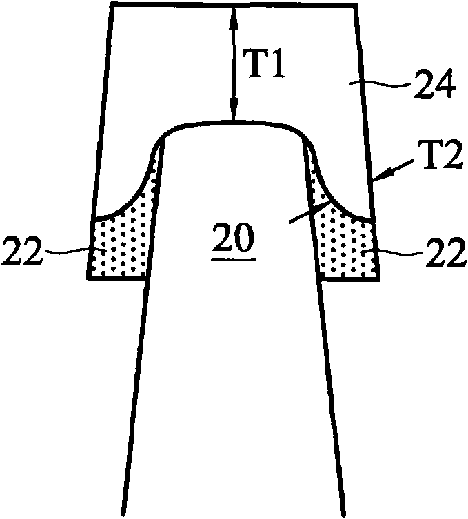
technical field [0001] The invention relates to an integrated circuit structure, in particular to a Fin Field Effect Transistor (FinFET). Background technique [0002] With increasing scaling of integrated circuits and progressively higher demands on integrated circuits, transistors must have higher drive currents and progressively smaller dimensions. Thus, fin field effect transistors (finfield-effect transistors, FinFET) are developed. Fin Field Effect Transistors (FinFETs) have increased channel widths, and the channel includes portions formed on the sidewalls of the fin and on the top surface of the fin. Since the drive currents of the transistor are proportional to the channel width, the drive current can be increased. [0003] Similar to a planar transistor, source and drain silicides may be formed on the source and drain regions of FinFETs. figure 1 A cross-sectional view of a source / drain region of a Fin Field Effect Transistor (FinFET) is disclosed. The source / d...

Claims


Application Information

Patent Timeline
Patent Type & Authority Patents(China)
IPC IPC(8): H01L29/78H01L29/06H01L29/41
CPCH01L29/785H01L29/66795H01L2029/7858H01L29/41791H01L27/1211H01L29/6681
Inventor 李宗霖叶致锴
Owner TAIWAN SEMICON MFG CO LTD
Learn More