A high-power high-brightness light-emitting diode chip and its manufacturing method

A technology of light-emitting diodes and manufacturing methods, which is applied in the direction of semiconductor devices, electrical components, circuits, etc., can solve the problem of weak coupling between photonic crystals and low-level waveguides, and does not fundamentally solve the problems of LED heat dissipation and current congestion, so as to reduce current congestion phenomenon, improvement of light extraction efficiency, and improvement of heat dissipation characteristics

Active Publication Date: 2011-12-21
QINGDAO TECHNOLOGICAL UNIVERSITY
View PDF4 Cites 6 Cited by
  • Summary
  • Abstract
  • Description
  • Claims
  • Application Information

AI Technical Summary

Problems solved by technology

[0003] (1) Low luminous efficiency;
[0004] (2) Low power;
[0005] (3) High cost
The existing photonic crystal LED mainly forms a photonic crystal structure on the upper surface of the LED. However, the surface photonic crystal LED structure has the following problems: (1) The coupling between the photonic crystal and the low-order waveguide light is weak, and it is difficult to realize the coupling of the low-order waveguide light. (2) During the manufacturing process of surface photonic crystals, the etching process may damage the active layer and affect the light extraction efficiency; (3) Compared with the planar LED structure, the manufacture of ohmic electrodes is difficult, and the current distribution is uneven, which affects the electrical characteristic
The traditional front-mounted structure LED is the most popular in the market, with low production cost, but there are disadvantages such as poor thermal conductivity (especially the sapphire substrate structure); the flip-chip structure LED is represented by Philips Lumileds, but it does not fundamentally solve the heat dissipation of the LED , current unevenness (current congestion), life expectancy and other issues; the two electrodes of the vertically structured LED chip are on both sides of the LED epitaxial layer, and the current Almost all flow vertically through the epitaxial layer of the LED, and very little current flows laterally, which can improve the current distribution problem of the planar structure, improve the luminous efficiency, and also solve the shading problem of the P pole, and increase the light-emitting area of ​​the LED

Method used


Image

  • A high-power high-brightness light-emitting diode chip and its manufacturing method
  • A high-power high-brightness light-emitting diode chip and its manufacturing method
  • A high-power high-brightness light-emitting diode chip and its manufacturing method

Examples


Embodiment 1

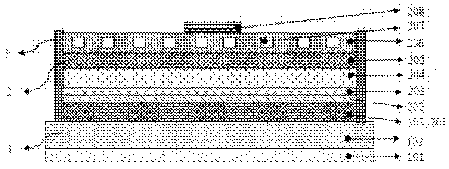
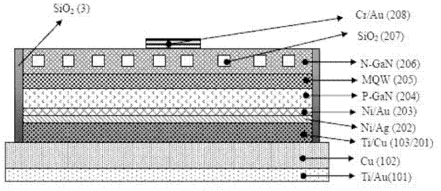
[0102] With metal copper (Cu) as the metal substrate 1, the vertical structure GaN-based embedded quasi-photonic crystal LED is the embodiment 1, and its specific structural diagram is as follows image 3 shown. Metal substrate 1 vertical structure GaN-based embedded quasi-photonic crystal LED includes from bottom to top: Ti / Au P-type ohmic contact electrode 101; metal Cu transfer metal substrate 102; Ti / Cu material metal bonding layer I103 and metal Bonding layer II201; metal reflective layer 202 of Ni / Ag; current spreading and P-type ohmic contact layer 203 of Ni / Au; P-type semiconductor layer 204 of P-GaN; 5-layer InGaN / GaN multiple quantum well (MQW) light emitting Layer 205; an embedded quasi-photonic crystal structure N-type semiconductor layer 206 of N-GaN; a quasi-photonic crystal structure SiO embedded in the N-type semiconductor layer 206 2 Nano dielectric pillar 207; N-type ohmic contact electrode 208 of Cr / Au; SiO 2 Passivation protection layer 3.

[0103] The m...

Embodiment 2

[0138] like Figure 7 , Figure 8 As shown, the present embodiment is similar to Embodiment 1, and the difference is that the substrate 102 is a copper alloy; the current spreading layer of ITO and the P-type ohmic contact layer 203; the metal reflective layer 202 of Ag / Cu; silicon nitride (Si 3 N 4 ) passivation protection layer 3. The characteristic structure of the quasi-photonic crystal structure embedded in the N-type semiconductor layer 206 is a 12-fold sunflower-type two-dimensional quasi-photonic crystal structure 514. The average diameter of the air holes is 80nm, and the distance between the centers of the nearest air holes is about 200nm. Height 120nm.

[0139] Figure 9 In order to improve electrical characteristics, improve current congestion. To achieve uniform current distribution and increase the light output area, the N-type ohmic contact electrode 208 on the light output surface can adopt a patterned electrode structure.


PUM

PropertyMeasurementUnit
Thicknessaaaaaaaaaa
Thicknessaaaaaaaaaa
Thicknessaaaaaaaaaa

Abstract

The invention discloses a large-power high-brightness light-emitting diode (LED) chip and a production method thereof. The large-power high-brightness LED chip comprises a metal substrate. An LED epitaxial wafer into which a photonic quasi-crystal structure is embedded is arranged above the metal substrate. Passivating protection layers are arranged on the two sides of the epitaxial wafer. A metal bonding layer, a metal reflecting layer, a current expansion and P-type ohmic contact layer, a P-type semiconductor layer, a light emitting layer, an N-type semiconductor layer into which the photonic quasi-crystal structure is embedded, and an N-type ohmic contact electrode are sequentially arranged on the epitaxial wafer from the bottom to the top. The passivating protection layers are arranged on the two sides of the epitaxial layer above the metal substrate. The invention additionally discloses a production method for the chip. The invention solves the problems of low-efficiency light extraction and ineffective heat dissipation of the LED chip at the same time, overcomes the defects of a surface photonic crystal LED structure, and provides an effective solution to the development of large-power high-brightness LEDs.

Description

technical field [0001] The invention relates to a metal substrate vertical structure embedded quasi-photonic crystal LED chip and a manufacturing method, in particular to a high-power and high-brightness light-emitting diode chip and a manufacturing method, belonging to the field of semiconductor lighting technology and nano-optoelectronic devices. Background technique [0002] High-power, high-brightness LEDs have been used in many fields such as automotive lighting, indoor and outdoor general lighting, LCD backlighting light sources, etc. With the continuous improvement of power and brightness and the continuous reduction of costs, LEDs will eventually replace the existing general-purpose The lighting source has become a new generation of green light source. But at present, LED still faces the following challenging technical problems: [0003] (1) Low luminous efficiency; [0004] (2) Low power; [0005] (3) The cost is high. [0006] This seriously affects and restric...

Claims


Application Information

Patent Timeline
IPC IPC(8): H01L33/20H01L33/00
Inventor 兰红波丁玉成
Owner QINGDAO TECHNOLOGICAL UNIVERSITY
Why Eureka
Try Eureka