Electric test structure and method for measuring epitaxial graphic offset

A technology of testing structure and offset, which is applied in the field of epitaxy, can solve the problems of inaccurate compensation of epitaxy pattern offset and inability to effectively control registration errors, etc., and achieve the effect of reducing registration errors and high measurement accuracy

Active Publication Date: 2011-06-15
SHANGHAI INTEGRATED CIRCUIT RES & DEV CENT
View PDF7 Cites 2 Cited by
  • Summary
  • Abstract
  • Description
  • Claims
  • Application Information

AI Technical Summary

Problems solved by technology

[0007] The present invention aims at defects such as the inaccurate compensation of the offset of the epitaxial pattern in the prior art and the inability to effectively control the registration error of the post-extended pattern and the pre-extended pattern, and provides an electrical test for measuring the offset of the epitaxial pattern structure

Method used


Image

  • Electric test structure and method for measuring epitaxial graphic offset
  • Electric test structure and method for measuring epitaxial graphic offset
  • Electric test structure and method for measuring epitaxial graphic offset

Examples


Embodiment Construction

[0033] In order to illustrate the technical content, structural features, achieved goals and effects of the present invention in detail, the following will be described in detail in conjunction with the embodiments and accompanying drawings.

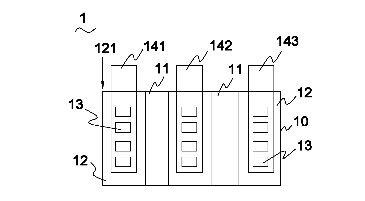
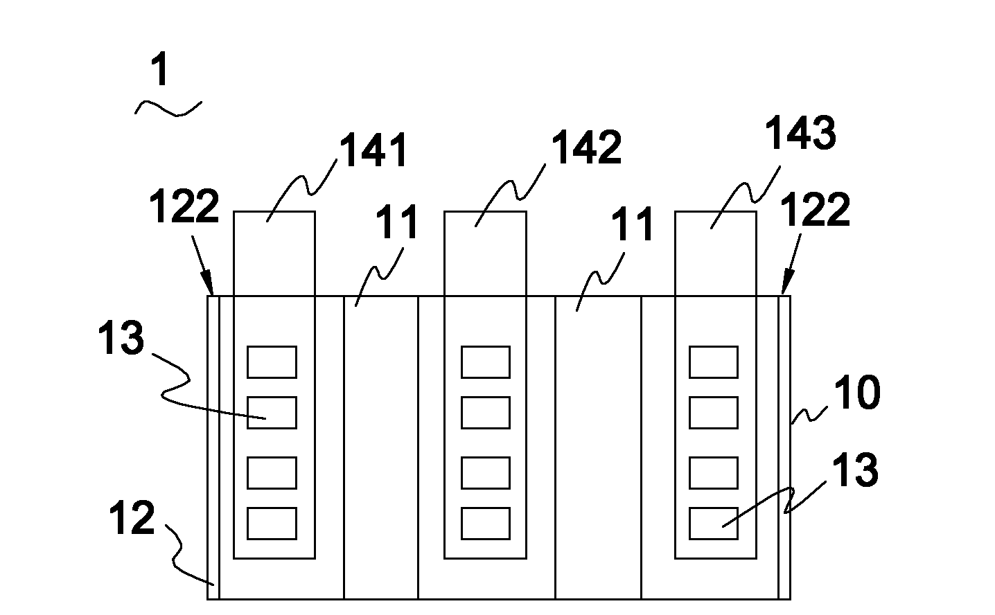
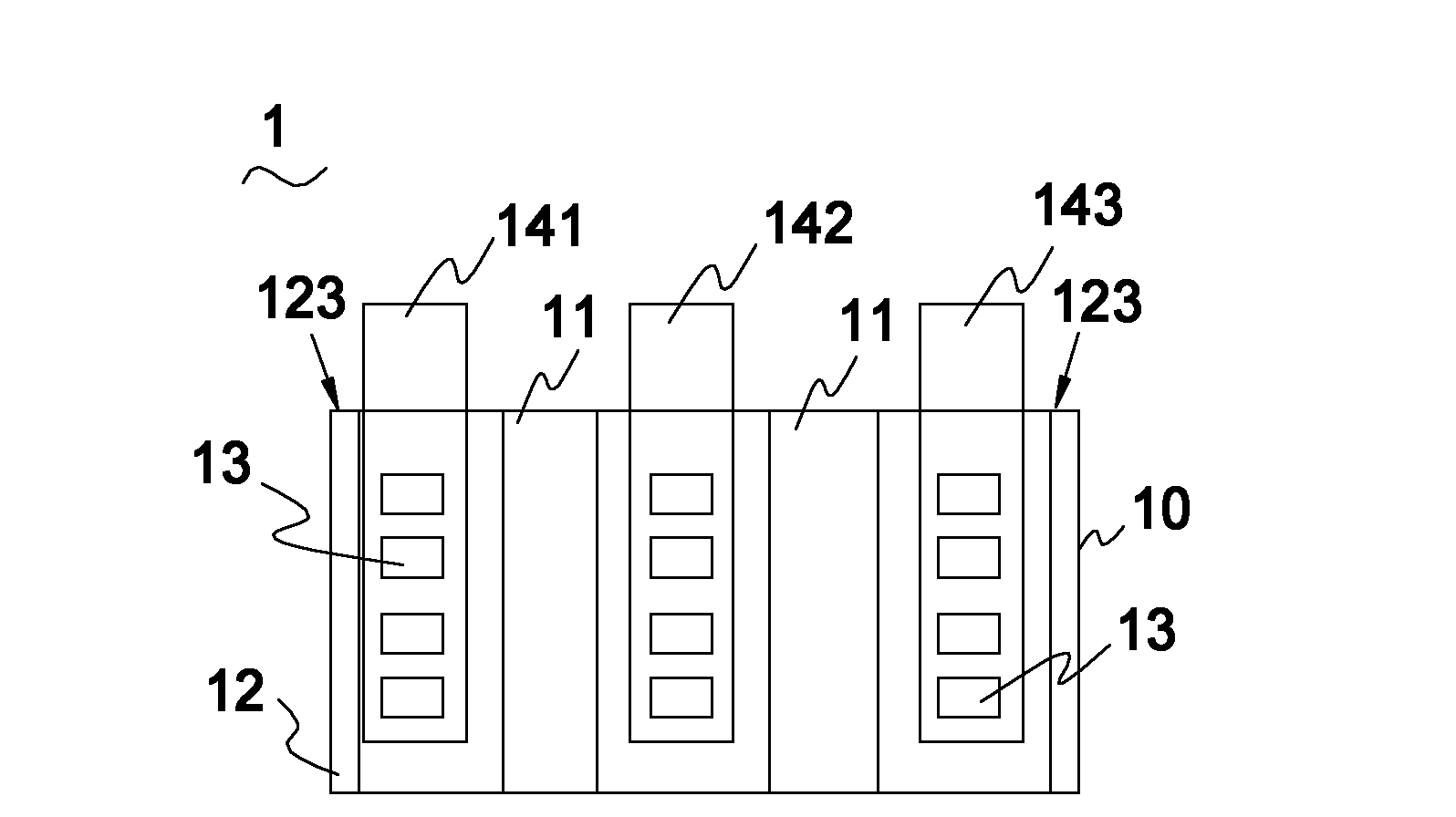
[0034] see Figure 1 to Figure 10 , Figure 1 to Figure 10 Shown is a schematic diagram of an electrical test structure 1 for measuring epitaxial pattern offset. The electrical test structure 1 includes diffusion of ions of the second conductivity type on the surface of a semiconductor substrate (not shown) having ions of the first conductivity type, so as to form buried ions of the second conductivity type on the surface of the semiconductor substrate. Layer 10. An epitaxial layer 11 having ions of the second conductivity type is epitaxially formed on the surface of the semiconductor substrate having the buried layer 10 . The buried layer 10 is located between the semiconductor substrate and the epitaxial layer 11 .

[0035] A plura...


PUM


Abstract

The invention relates to an electric test structure for measuring epitaxial graphic offset, comprising a buried layer formed on the surface of a semiconductor substrate, an epitaxial layer formed on the surface of the semiconductor substrate, a plug region equidistantly which is formed in the epitaxial layer on the surface of the semiconductor substrate and has a preset offset different with the buried layer along the same direction, a contact hole formed on the surface of the plug region as well as a first conductive connection, a second conductive connection and a third conductive connection which are sequentially formed at the contact hole on the adjacent plug region. The method for measuring the epitaxial graphic offset comprises the step of respectively carrying out an electric test on the electric test structure with different preset offsets. In the invention, the electric test structure is utilized to measure the epitaxial graphic offset, not only is the measuring accuracy higher, but also the registration error of a graph after extension to the graph before extension can be effective reduced.

Description

technical field [0001] The invention relates to an epitaxy process in the manufacture of integrated circuits, in particular to an electrical test structure and method for measuring the offset of epitaxy patterns. Background technique [0002] In the bipolar semiconductor manufacturing process, the method of growing a single crystal semiconductor thin film on the surface of a silicon substrate is called epitaxy. There are many benefits to epitaxial growth on the initial wafer. For one, the epitaxial layer does not need to have the same doping type as the underlying wafer. For example, in a bipolar process, an N-type epitaxial layer can be grown on a P-type substrate. Second, unlike CZ silicon, epitaxial silicon is not contaminated by oxygen or carbon elements. [0003] At the same time, a buried layer is also allowed to be formed in the epitaxial layer. The N+ buried layer becomes a critical step in most bipolar processes because it enables the fabrication of vertical NPN...

Claims


Application Information

Patent Timeline
Patent Type & Authority Applications(China)
IPC IPC(8): H01L21/66
Inventor 顾学强
Owner SHANGHAI INTEGRATED CIRCUIT RES & DEV CENT
Why Eureka
Try Eureka