Organic light emitting diode device

A light-emitting diode, an organic technology, applied in the field of organic light-emitting diode devices, capable of solving problems such as deterioration of white light emission stability

Active Publication Date: 2011-06-15
SAMSUNG DISPLAY CO LTD
View PDF5 Cites 23 Cited by
  • Summary
  • Abstract
  • Description
  • Claims
  • Application Information

AI Technical Summary

Problems solved by technology

[0008] In the alternatives described above, since the color characteristics and efficiency of each emission layer may vary depending on the characteristics of the emission layer, the stability of white light emission may deteriorate

Method used


Image

  • Organic light emitting diode device
  • Organic light emitting diode device
  • Organic light emitting diode device

Examples


Embodiment Construction

[0034] The present disclosure will be described more fully hereinafter with reference to the accompanying drawings, in which exemplary embodiments are shown. As those skilled in the art would realize, the described embodiments may be modified in various ways, all without departing from the spirit or scope of the present disclosure.

[0035] In the drawings, the thickness of layers, films, panels, regions, etc., are exaggerated for clarity. Like reference numbers generally refer to like elements throughout the specification. It will be understood that when an element such as a layer, film, region, or substrate is referred to as being "on" another element, it can be directly on the other element or intervening layers may also be present.

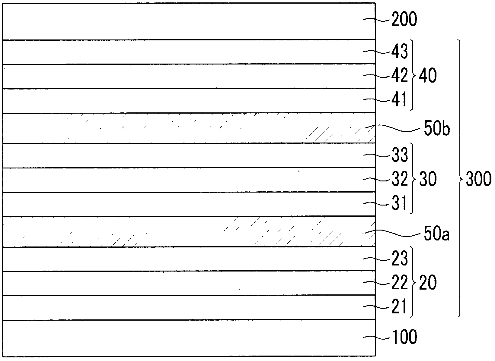
[0036] refer to figure 1 An organic light emitting diode device according to an exemplary embodiment is described in detail.

[0037] figure 1 is a cross-sectional view of an organic light emitting diode device according to an exemplary em...


PUM


Abstract

An organic light emitting diode device is disclosed. The organic light emitting diode device includes a light emitting layer which includes at least two blue light emitting units and at least one orange light emitting unit. Such a device exhibits excellent color characteristic and high luminance and efficiency, as well as a longer life span due to the materials used. In particular, the white light represents color of high color purity after it passes through a color filter.

Description

technical field [0001] Embodiments relate to organic light emitting diode devices. Background technique [0002] Recently, organic light emitting diode (OLED) devices have drawn attention as display devices and as lighting devices. [0003] An OLED device generally includes two electrodes and an emissive layer between the two electrodes, electrons are injected from one electrode, holes are injected from the other electrode, and the electrons and holes recombine in the emissive layer to generate excitons, These excitons release energy and emit light. [0004] Since the OLED device emits light without an additional light source, it has low power consumption, better response speed, viewing angle, and contrast. [0005] An organic light emitting diode device generally includes a plurality of sub-pixels for each pixel, such as a red sub-pixel, a blue sub-pixel, and a green sub-pixel, and expresses full colors by combining the sub-pixels. [0006] The red, blue, and green sub-p...

Claims


Application Information

Patent Timeline
Patent Type & Authority Applications(China)
IPC IPC(8): H01L27/32H01L51/00H01L51/54H01L25/04
CPCH01L51/5036H01L27/3213H10K59/351H10K50/125H05B33/14H10K50/00
Inventor 李晟熏田村真一郎宋正培
Owner SAMSUNG DISPLAY CO LTD
Why Eureka
Try Eureka