Supercharge Your Innovation With Domain-Expert AI Agents!

Flash memory-interface

A technology of flash memory and main memory, which is applied in instruments, electrical digital data processing, etc., and can solve the problems that flash memory devices are not compatible with other devices or processors, and flash memory cannot be modified and accessed quickly.

Inactive Publication Date: 2011-06-22
NXP BV
View PDF7 Cites 20 Cited by
  • Summary
  • Abstract
  • Description
  • Claims
  • Application Information

AI Technical Summary

Problems solved by technology

In many cases, flash memory devices are not compatible with certain types of other devices or processors
In addition, many forms of flash memory cannot be modified to the fast access required or desired in a particular application
[0004] These and other issues continue to challenge the utilization of serial flash memory

Method used


Image

  • Flash memory-interface
  • Flash memory-interface
  • Flash memory-interface

Examples


Embodiment Construction

[0019] The invention is believed to be applicable to various types of processors, devices and arrangements for computer memory applications. While the invention is not necessarily so limited, aspects of the invention can be understood by discussing examples using this context.

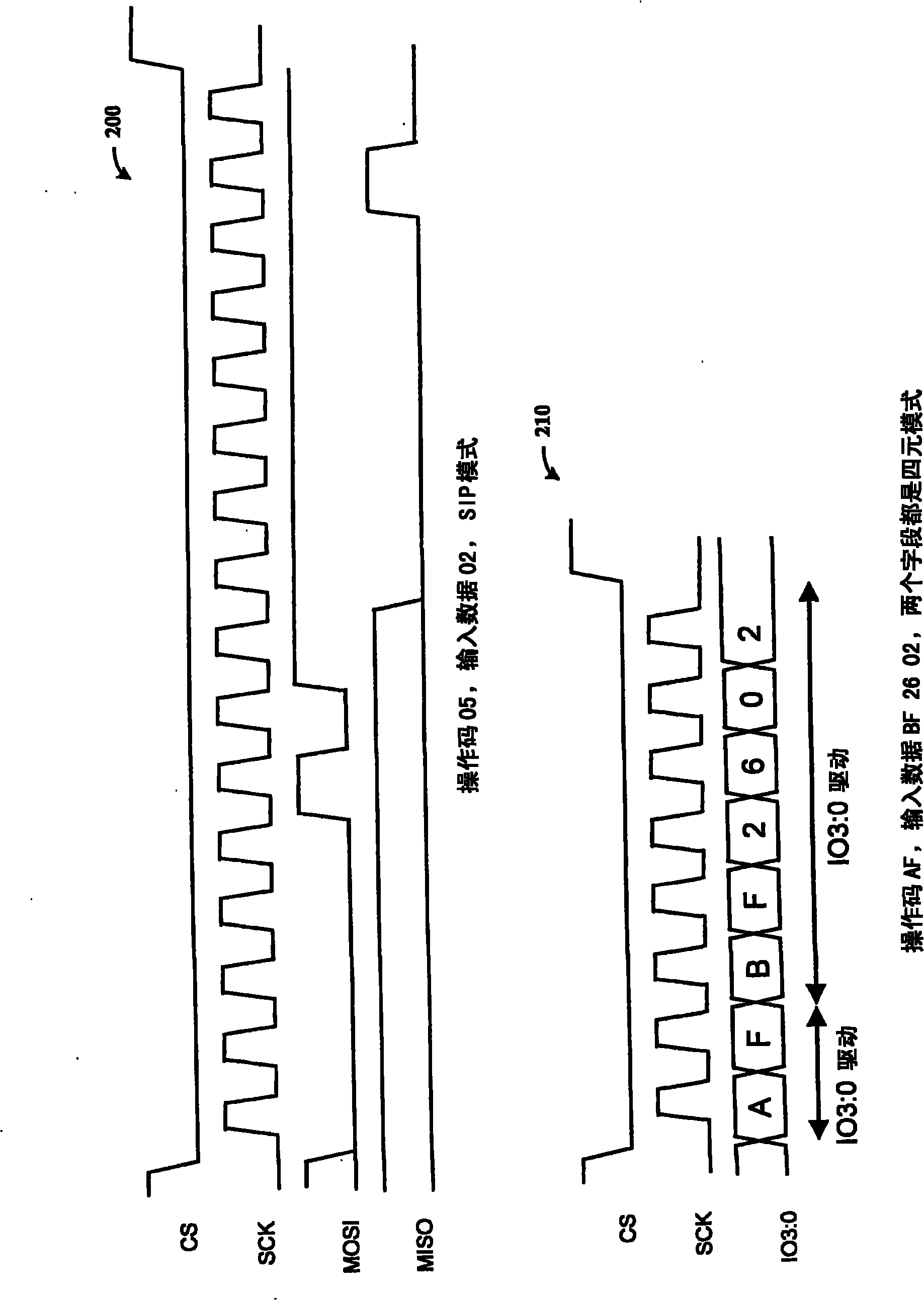
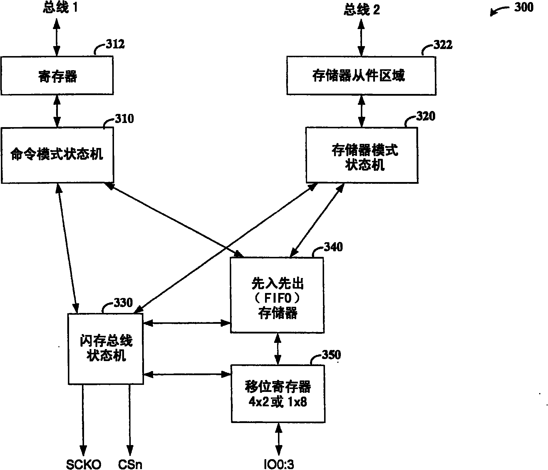
[0020] In connection with various example embodiments, the flash memory interface is configured to interface between a computer processor (CPU) (and optionally its memory controller) and the flash memory circuit for writing data to the flash memory circuit, And read data from the flash memory circuit. The flash memory interface includes: a communication port for communicating with the flash memory circuit; a first-in-first-out (FIFO) type buffer for storing data transferred to and from the flash memory circuit; and a controller configured to respond to the The CPU or memory controller controls writing of data to and reading data from the flash memory circuit.

[0021] The flash memory interface is co...


PUM


Abstract

Flash-type memory access and control is facilitated (e.g., as random-access memory). According to an example embodiment, an interface communicates with and controls a flash memory circuit over a peripheral interface bus. The interface uses a FIFO buffer coupled to receive data from and store data for the flash memory circuit and to provide access to the stored data. An interface controller communicates with the flash memory circuit via the peripheral interface bus to initialize the flash memory circuit and to access data thereto, in response to requests from a processor. In some applications, the flash memory circuit is initialized by sending commands to it. The interface may be placed into a read-only mode in which data in the flash memory is accessed as part of main (computer) processor memory, using the FIFO to buffer data from the flash.

Description

technical field [0001] The present invention relates generally to memory devices, and more particularly to memory devices having a flash-type interface. Background technique [0002] Flash memory is a non-volatile type of erasable and rewritable memory that has experienced great success due to its relatively inexpensive nature. In many cases, flash memory is erased and programmed in larger blocks. Implementations of flash memory have included external storage such as memory cards and flash drives, as well as internal storage such as solid-state storage for handheld or mobile devices. [0003] Flash memory devices operate in various ways. In many applications, command mode is used for operations such as erase and program, while memory mode is used for reading data from flash memory. In some applications, flash memory devices use a half-duplex command-driven Serial Peripheral Interface (SPI) protocol for device setup / initialization, and then move to a half-duplex command-dr...

Claims


Application Information

Patent Timeline
Patent Type & Authority Applications(China)
IPC IPC(8): G06F13/40G06F13/16
CPCG06F13/4234
Inventor 克雷格·麦肯纳普里特维·纳加拉杰罗伯·科萨诺
Owner NXP BV
Features
  • R&D
  • Intellectual Property
  • Life Sciences
  • Materials
  • Tech Scout
  • Unparalleled Data Quality
  • Higher Quality Content
  • 60% Fewer Hallucinations
Learn More