Thermally-assisted magnetic writing using an oxide layer and current-induced heating

a technology of magnetic writing and oxide layer, applied in the field of current-induced heating, can solve the problems of limited scalability beyond the 65 nm technology node, unsuitable replacement for volatile memories such as dram or sram, and very slow flash speed

Inactive Publication Date: 2004-08-03
GLOBALFOUNDRIES U S INC
View PDF4 Cites 183 Cited by
  • Summary
  • Abstract
  • Description
  • Claims
  • Application Information

AI Technical Summary

Benefits of technology

There are numerous disadvantages to both OUM and MTJ-MRAM technologies. For OUM, write times are rather slow (about 50 ns) due to the crystallization period required and has limited write cycles (about 1013) due to the repeated melting of the media MTJ-MRAM can be more than ten times faster and can have an almost unlimited number of write cycles. However, MTJ-MRAM may suffer from a large cell size due to the more complicated write process and inadvertent switching of elements elsewhere on the bit or word lines due to materials variations and the half-select addressing scheme. The most serious limitation, however, is that MTJ-MRAM suffers from poor scaling of the current density necessary to produce the write field as the wires are made smaller and the coercivity of the soft electrode is increased to avoid superparamagnetism. For example, to scale to the 20 nm node, a cube-shaped magnetic bit needs an anisotropy energy (Ku) of Ku=50 kBT / V=2.8.times.105 ergs / cm3 where T / V is temperature over volume. Assuming a magnetization of 1000 emu / cm3, the anisotropy field (Hk) would need to be Hk=2 Ku / M=570 Oe where M is magnetization. In the Stoner-Wohlfarth model of magnetic reversal, we can take Hk to be approximately equal to the field necessary for fast switching. For 20 nm.times.20 nm bit and word wires (at 45 degrees to the magnetic axis) to produce 570 Oe 20 nm from their centers, the current density would need to be at least j=(5 / 21 / 2)Hk / d=1.times.109 A / cm2 where d is the height and width. Assuming the copper bit and word lines are 256 cells long (10 mm), the voltage would be V=jrL=2 volts, where j is the current density, r is the resistivity, and L is the length of the line. The power would be P=2 Vjd2=16 mW. Problems of electromigration and power dissipation at such large current densities seem to preclude the practical use of field-induced MTJ writing at the 20 nm node (and perhaps well before this node is reached).

Problems solved by technology

Unfortunately, Flash is very slow and has a very limited number of write cycles (about 10.sup.6) before failure, making it unsuitable as a replacement for volatile memories such as DRAM or SRAM.
It is also believed to have limited scalability beyond the 65 nm technology node.

Method used


Image

  • Thermally-assisted magnetic writing using an oxide layer and current-induced heating
  • Thermally-assisted magnetic writing using an oxide layer and current-induced heating
  • Thermally-assisted magnetic writing using an oxide layer and current-induced heating

Examples


Embodiment Construction

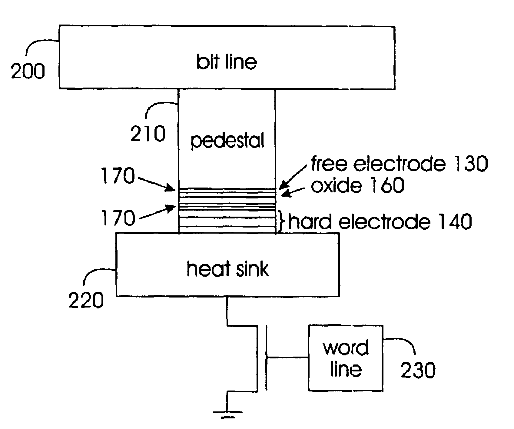
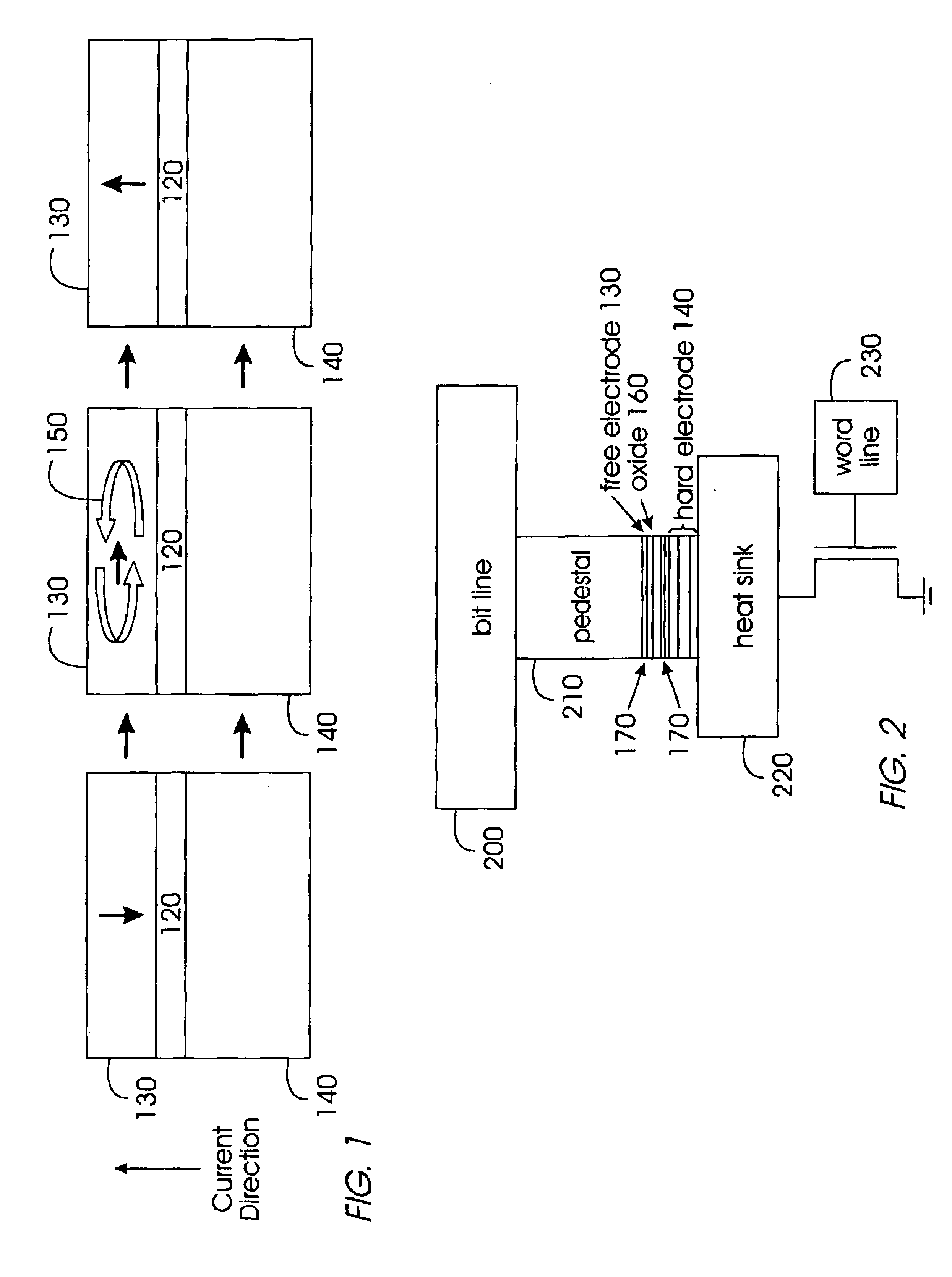
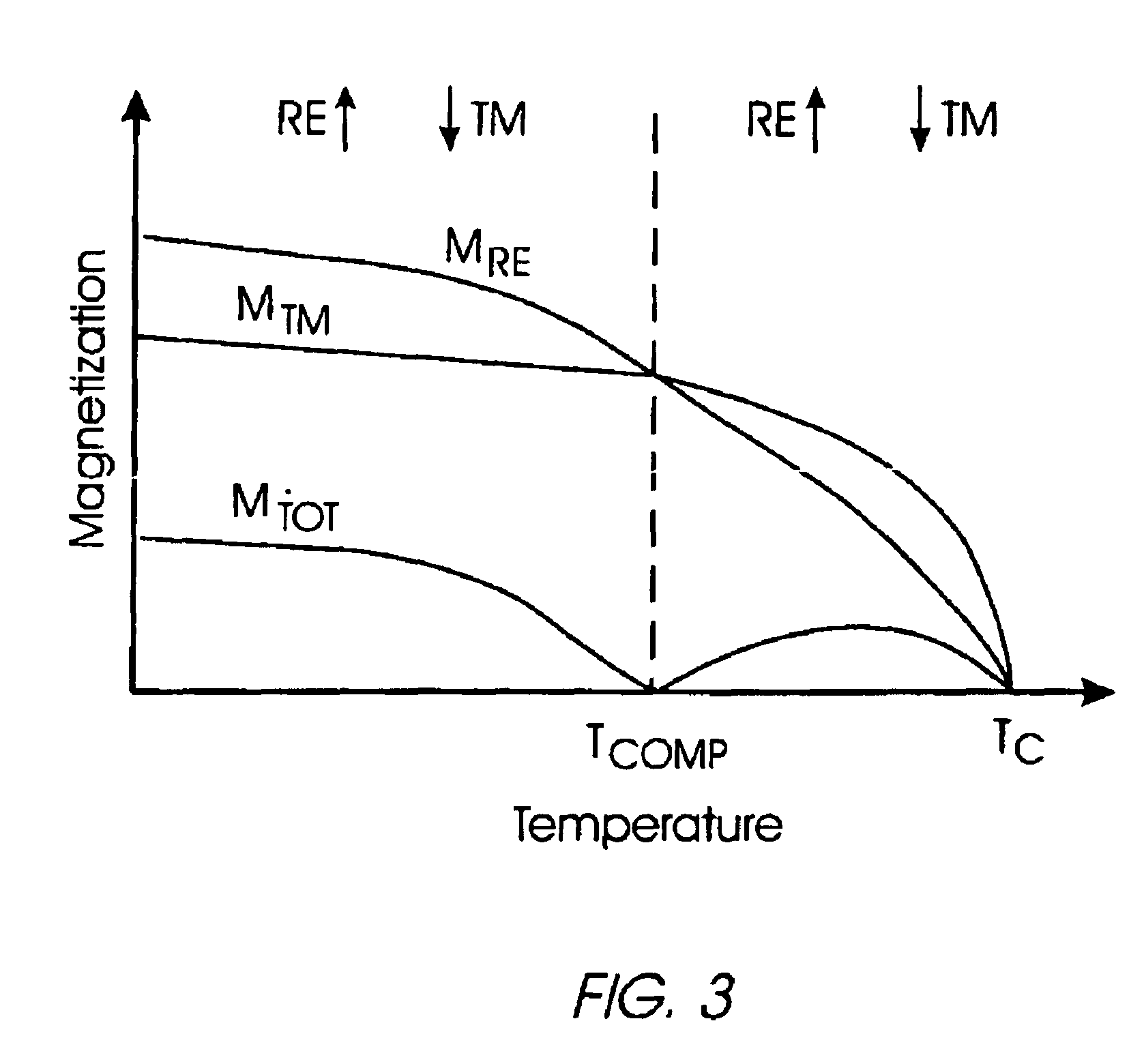
With the invention, thermally-assisted magnetic writing is accomplished by passing current through an ultra-low resistance oxide layer adjacent or near to a free electrode to be switched. Current-induced heating lowers the anisotropy of the free electrode and reduces the current density required for field or spin-transfer-based writing. In one embodiment of the invention, the resistance through the oxide layer in on the order 4 .OMEGA.-.mu.m.sup.2, the free electrode is comprising of Tb.sub.x Fe.sub.y based alloy, and switching is induced by spin-transfer torque with thermal assist. Thus, the invention provides a non-volatile MRAM memory device with a large number of read and write cycles, current-controlled switching, excellent scalability, ultra-fast switching speeds, very small bit cell, low voltage, low power, and optimal resistance for CMOS integration.

As mentioned above, the non-volatile memory chip market is today dominated by Flash technology. Unfortunately, Flash is very sl...


PUM

PropertyMeasurementUnit
melting temperatureaaaaaaaaaa
resistanceaaaaaaaaaa

Abstract

A method and structure for a non-volatile magnetic random access memory (MRAM) device that has a stable magnetic electrode, an oxide layer adjacent the stable magnetic electrode, and a free magnetic electrode. The oxide layer is between the stable magnetic electrode and the free magnetic electrode. In the invention, a conductor is connected to a stable magnetic electrode. The oxide layer has a resistance at levels to allow sufficient power dissipation to lower the anisotropy of the free magnetic electrode through current induced heating. Current-induced heating is used in combination with spin-transfer torque or a magnetic field to switch the free magnetic electrode.

Description

1. Field of the InventionThe present invention generally relates to thermally-assisted magnetic writing and more particularly to current-induced heating in magnetic random access memory devices.2. Description of the Related ArtThe non-volatile memory chip market is today dominated by Flash technology. Unfortunately, Flash is very slow and has a very limited number of write cycles (about 10.sup.6) before failure, making it unsuitable as a replacement for volatile memories such as DRAM or SRAM. It is also believed to have limited scalability beyond the 65 nm technology node. Therefore, there is a need for a new type of non-volatile memory.The invention provides a non-volatile magnetic random access memory (MRAM) device that has a stable magnetic electrode comprising of one or more layers, an oxide layer, and a free magnetic electrode comprising of one or more layers. When the oxide is used as a barrier, the stable and free magnetic electrodes are adjacent to the oxide. In the oxide de...

Claims


Application Information

Patent Timeline
Patent Type & Authority Patents(United States)
IPC IPC(8): G11C11/15G11C11/02H01F10/32H01F41/30H01L21/8246H01L27/105H01L27/22H01L43/08
CPCB82Y10/00B82Y25/00G11C11/15H01L43/08H01F10/3254H01F41/305H01L27/228G11C11/1675H10B61/22H10N50/10
Inventor STIPE, BARRY C.
Owner GLOBALFOUNDRIES U S INC
Why Eureka
Try Eureka