Static random access memory (SRAM) cell and method for forming same

a random access memory and cell technology, applied in the field of static random access memory (sram) cells, can solve the problems of preventing the use of sram in devices that require very small sram cells, affecting the use of fin field effect transistors (finfets) in the sram, and the processing requirements of conventional sram cells

Inactive Publication Date: 2011-08-23
TAIWAN SEMICON MFG CO LTD
View PDF51 Cites 182 Cited by
  • Summary
  • Abstract
  • Description
  • Claims
  • Application Information

AI Technical Summary

Benefits of technology

A conventional 6T SRAM layout may be used in 90 nm, 65 nm, 45 nm, and 32 nm technology, but problems occur that can prevent using the layout for smaller technology. For instance, as the cell size becomes smaller, the individual components, such as the active areas of the transistors, the intra-cell connections, and contacts, would naturally need to become smaller. Unfortunately, current lithography and etching techniques limit the size of individual components. Hence, once the individual components decrease to the smallest possible size, if the cell size continues to decrease, the components will cause a greater density within the cell and may overlay other components. Any overlay would lead to a short circuit between different components causing device failure.

Problems solved by technology

However, the size of the SRAM cell is limited by problems encountered in processing.
This prevents the use of SRAM in devices that require very small SRAM cells.
Further, processing requirements of conventional SRAM cells hinder the use of fin field effect transistors (FinFETs) in the SRAM.
A conventional 6T SRAM layout may be used in 90 nm, 65 nm, 45 nm, and 32 nm technology, but problems occur that can prevent using the layout for smaller technology.
Unfortunately, current lithography and etching techniques limit the size of individual components.
Hence, once the individual components decrease to the smallest possible size, if the cell size continues to decrease, the components will cause a greater density within the cell and may overlay other components.
Any overlay would lead to a short circuit between different components causing device failure.
These active zags generally create problems with current mismatch between the pull-down and pull-up transistors and leakage current between the pass-gate and pull-down transistors.
The problems generally arise because of weaknesses in processing sharp corners, such as those of the active zag.
Also, a strong electric field around the corner may cause leakage problems.
As a result, if the contact cannot be etched any smaller, the contact may also be a limiting factor; otherwise, overlay of the contact with the gate electrode spacers may result and adversely affect performance.
The length of this dimension can result in long bitlines that can increase line capacitance and can slow the performance of the SRAM cell.
The multiple etching steps may generally create more costs in processing and may cause more processing control problems.
Furthermore, the conventional layout also is not generally compatible with the process for building FinFETs.
Generally FinFETs and tri-gate transistors need to be the same width in SRAM cells, but by making the transistors the same width in the conventional layout, SRAM issues, such as instability of the SRAM due to a beta-ratio that is too low, may arise.

Method used


Image

  • Static random access memory (SRAM) cell and method for forming same
  • Static random access memory (SRAM) cell and method for forming same
  • Static random access memory (SRAM) cell and method for forming same

Examples


Embodiment Construction

The making and using of the present embodiments are discussed in detail below. It should be appreciated, however, that the present invention provides many applicable inventive concepts that can be embodied in a wide variety of specific contexts. The specific embodiments discussed are merely illustrative of specific ways to make and use the invention, and do not limit the scope of the invention.

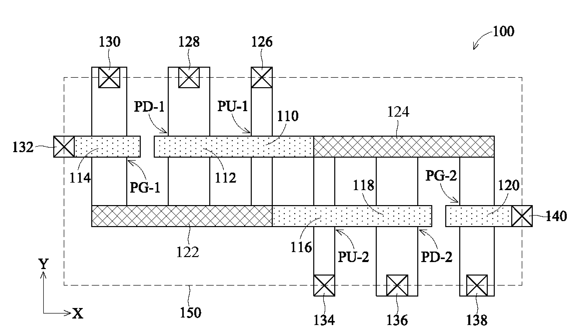
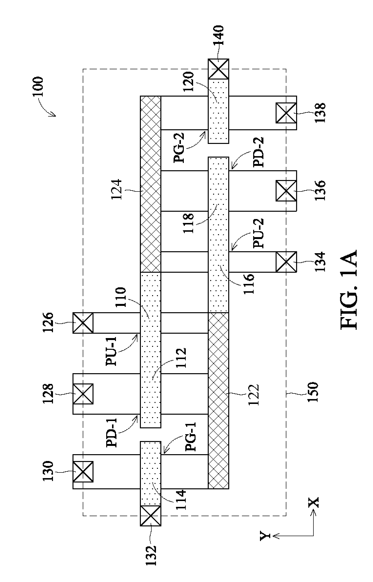
The present invention will be described with respect to embodiments in a specific context, namely a 6T SRAM layout and a dual port SRAM layout. The invention may also be applied, however, to any kind of SRAM cell layout, including 10T SRAM layouts.

FIG. 1A shows a layout of a 6T SRAM cell 100 in accordance with embodiments of the invention. The memory cell layout 100 comprises a first pass-gate transistor PG-1, a second pass-gate transistor PG-2, a first pull-down transistor PD-1, a second pull-down transistor PD-2, a first pull-up transistor PU-1, and a second pull-up transistor PU-2 disposed ...


PUM


Abstract

In accordance with an embodiment of the present invention, a static random access memory (SRAM) cell comprises a first pull-down transistor, a first pull-up transistor, a first pass-gate transistor, a second pull-down transistor, a second pull-up transistor, a second pass-gate transistor, a first linear intra-cell connection, and a second linear intra-cell connection. Active areas of the transistors are disposed in a substrate, and longitudinal axes of the active areas of the transistors are all parallel. The first linear intra-cell connection electrically couples the active area of the first pull-down transistor, the active area of the first pull-up transistor, and the active area of the first pass-gate transistor to a gate electrode of the second pull-down transistor and a gate electrode of the second pull-up transistor. The second linear intra-cell connection electrically couples the active area of the second pull-down transistor, the active area of the second pull-up transistor, and the active area of the second pass-gate transistor to a gate electrode of the first pull-down transistor and a gate electrode of the first pull-up transistor.

Description

TECHNICAL FIELDThe present invention relates generally to semiconductor devices and, more particularly, to a static random access memory (SRAM) cell and a method for creating a SRAM cell.BACKGROUNDStatic Random Access Memory (SRAM) is chosen as a reliable, proven technology for high-performance stand-alone memory devices or embedded memory devices. The distinct advantages of an SRAM include fast access speed, low power consumption, high noise margin, and process compatibility with a conventional CMOS fabrication process, among others. However, the size of the SRAM cell is limited by problems encountered in processing. This prevents the use of SRAM in devices that require very small SRAM cells. Further, processing requirements of conventional SRAM cells hinder the use of fin field effect transistors (FinFETs) in the SRAM. Thus, there is a need for a layout of an SRAM cell that obviates processing problems for small cell sizes and allows for the application of FinFETs in SRAM.A conven...

Claims


Application Information

Patent Timeline
Patent Type & Authority Patents(United States)
IPC IPC(8): H01L27/11H01L21/768
CPCH01L27/0207H01L27/11H01L27/0886H01L27/088H01L27/1104H10B10/12H10B10/00
Inventor YANG, LIE-YONGCHANG, FENG-MINGYANG, CHANG-TAWANG, PING-WEI
Owner TAIWAN SEMICON MFG CO LTD
Why Eureka
Try Eureka