Microfluidic large scale integration

a microfluidic and large-scale technology, applied in the field of microfluidic large-scale integration, can solve the problems of “tyranny of numbers, practical limit to the complexity of macroscopically assembled systems, and complex circuits quickly became very expensive to build and opera

Active Publication Date: 2006-12-05
MOTOROLA INC +1
View PDF74 Cites 189 Cited by
  • Summary
  • Abstract
  • Description
  • Claims
  • Application Information

AI Technical Summary

Benefits of technology

[0010]High-density microfluidic chips contain plumbing networks with thousands of micromechanical valves and hundreds of individually addressable chambers. These fluidic devices are analogous to electronic integrated circuits fabricated using large scale integration. A component of these networks is the fluidic multiplexor, which is a combinatorial array of binary valve patterns that exponentially increases the processing power of a network by allowing complex fluid manipulations with a minimal number of inputs. These integrated microfluidic networks can be used to construct the microfluidic analog of a comparator array and a microfluidic memory storage device resembling electronic random access memories.

Problems solved by technology

In the first part of the 20th century, engineers faced a problem commonly called the “Tyranny of Numbers”: there is a practical limit to the complexity of macroscopically assembled systems.
Using discrete components such as vacuum tubes, complex circuits quickly became very expensive to build and operate.
The transistor was invented at Bell Laboratories in 1947 and went on to replace the bulky vacuum tubes in circuits, but connectivity remained a problem.
Although engineers could in principle design increasingly complex circuits consisting of hundreds of thousands of transistors, each component within the circuit had to be hand-soldered: an expensive, labor-intensive process.
Adding more components to the circuit decreased its reliability as even a single cold solder joint rendered the circuit useless.
However, devices to date have lacked a method for a high degree of integration, other than simple repetition.

Method used


Image

  • Microfluidic large scale integration
  • Microfluidic large scale integration
  • Microfluidic large scale integration

Examples


Embodiment Construction

I. Microfabrication Overview

[0074]The following discussion relates to formation of microfabricated fluidic devices utilizing elastomer materials, as described generally in U.S. nonprovisional patent application Ser. No. 10 / 118,466 filed Apr. 5, 2002, Ser. No. 09 / 997,205 filed Nov. 28, 2001, Ser. No. 09 / 826,585 filed Apr. 6, 2001, Ser. No. 09 / 724,784 filed Nov. 28, 2000, and Ser. No. 09 / 605,520, filed Jun. 27, 2000. These patent applications are hereby incorporated by reference for all purposes.

1. Methods of Fabricating

[0075]Exemplary methods of fabricating the present invention are provided herein. It is to be understood that the present invention is not limited to fabrication by one or the other of these methods. Rather, other suitable methods of fabricating the present microstructures, including modifying the present methods, are also contemplated.

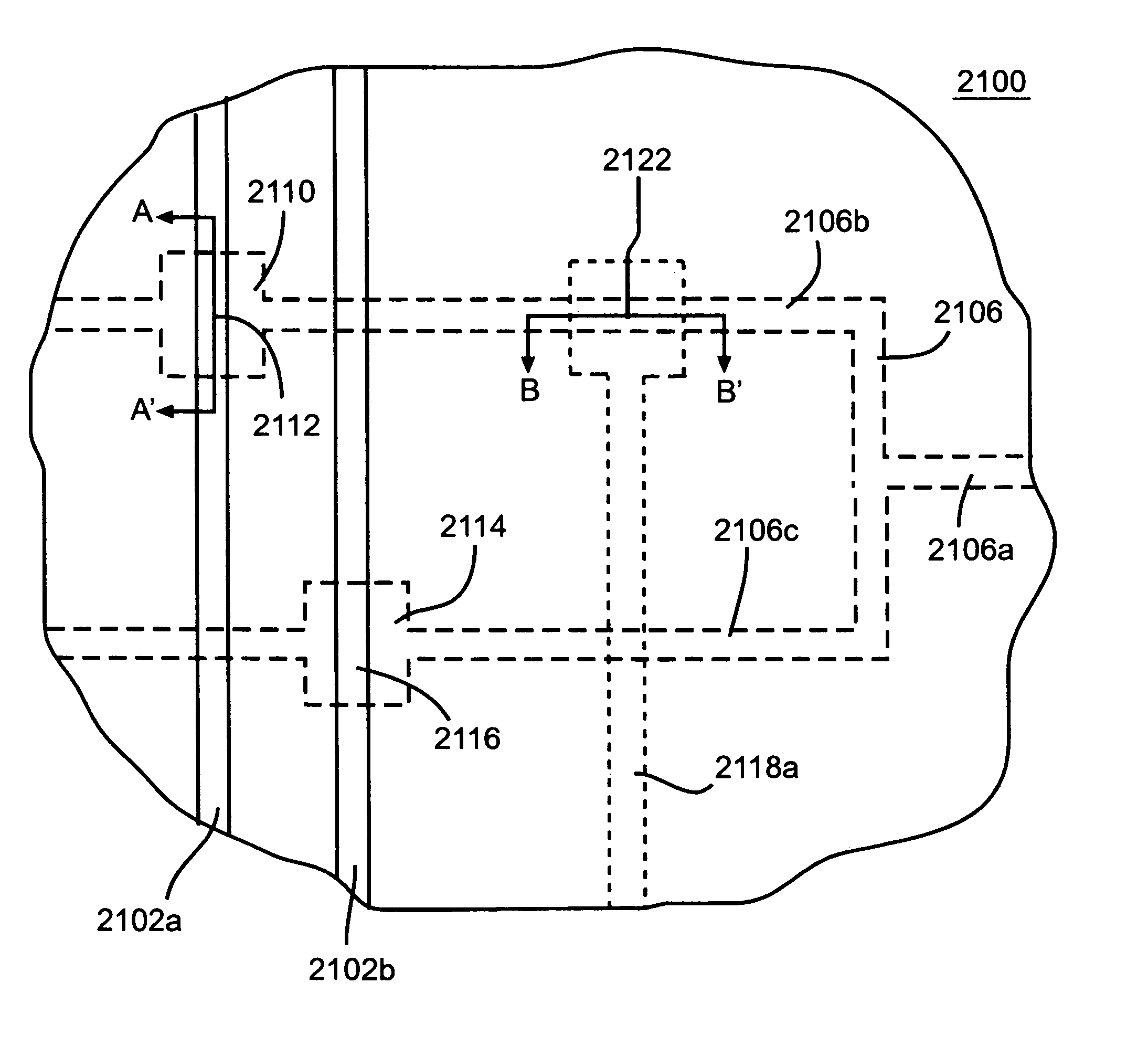
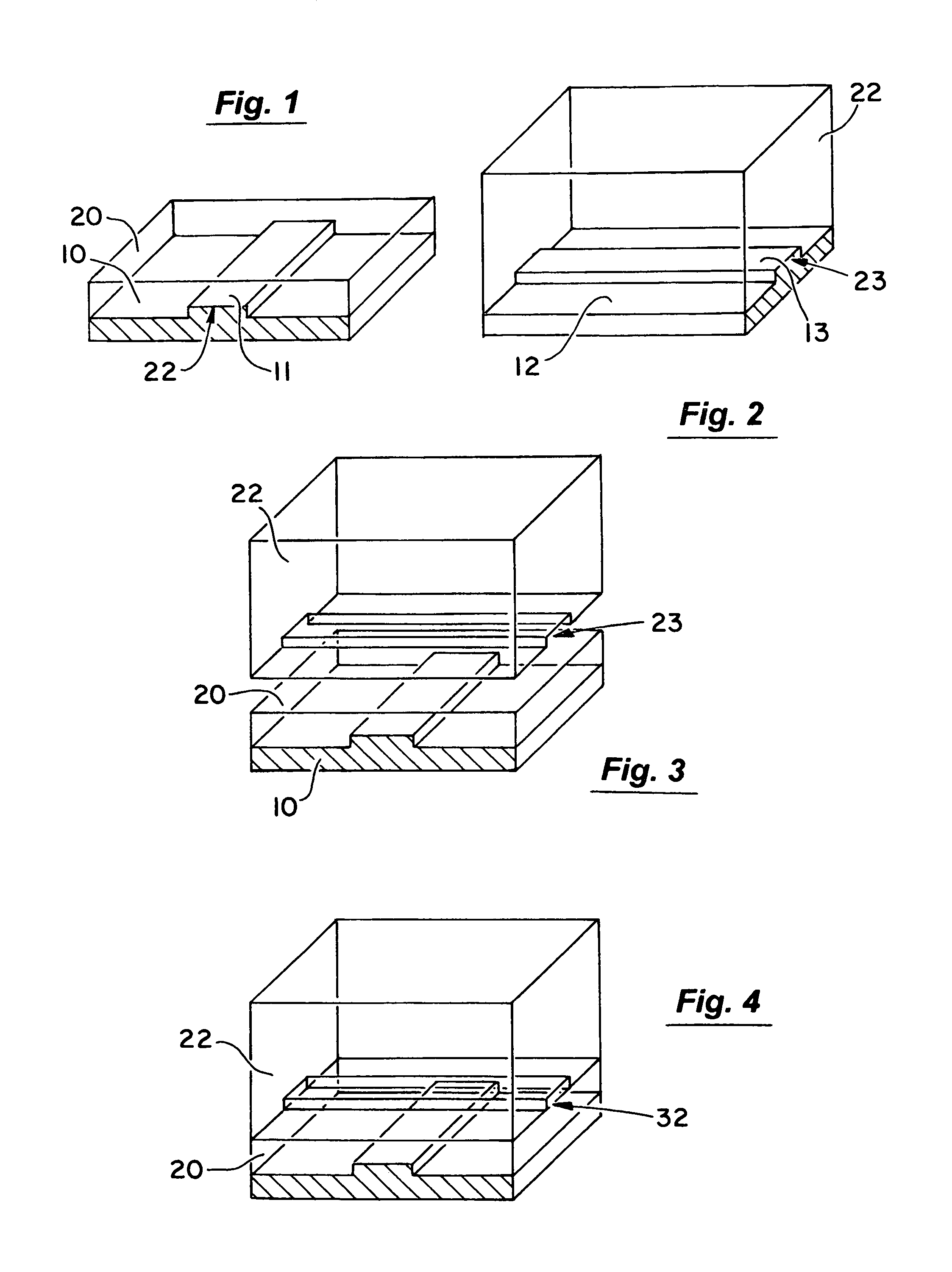
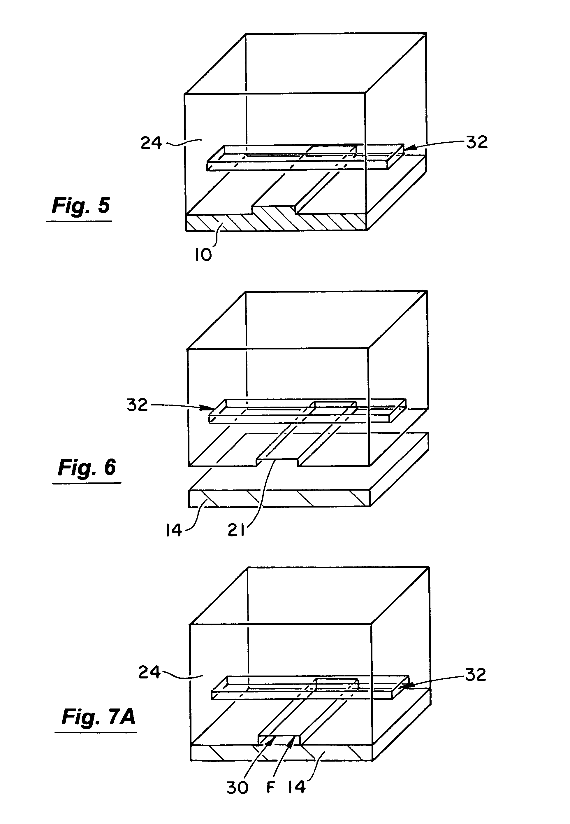
[0076]FIGS. 1 to 7B illustrate sequential steps of a first preferred method of fabricating the present microstructure, (which may be us...


PUM


Abstract

High-density microfluidic chips contain plumbing networks with thousands of micromechanical valves and hundreds of individually addressable chambers. These fluidic devices are analogous to electronic integrated circuits fabricated using large scale integration (LSI). A component of these networks is the fluidic multiplexor, which is a combinatorial array of binary valve patterns that exponentially increases the processing power of a network by allowing complex fluid manipulations with a minimal number of inputs. These integrated microfluidic networks can be used to construct a variety of highly complex microfluidic devices, for example the microfluidic analog of a comparator array, and a microfluidic memory storage device resembling electronic random access memories.

Description

CROSS-REFERENCE TO RELATED APPLICATIONS[0001]The instant patent application claims priority from U.S. provisional patent application Ser. No. 60 / 413,860 filed Sep. 25, 2002, hereby incorporated by reference for all purposes.STATEMENT AS TO RIGHTS TO INVENTIONS MADE UNDER FEDERALLY SPONSORED RESEARCH AND DEVELOPMENT[0002]Work described herein has been supported, in part, by NSF a grant from the Army Research Office (No. DAAD19-00-1-0392) and the DARPA Bioflips program. The United States Government may therefore have certain rights in the invention.BACKGROUND OF THE INVENTION[0003]In the first part of the 20th century, engineers faced a problem commonly called the “Tyranny of Numbers”: there is a practical limit to the complexity of macroscopically assembled systems. Using discrete components such as vacuum tubes, complex circuits quickly became very expensive to build and operate. The ENIAC I, created at the university of Pennsylvania in 1946, consisted of 19,000 vacuum tubes, weighe...

Claims


Application Information

Patent Timeline
Patent Type & Authority Patents(United States)
IPC IPC(8): F16K11/20F16K7/00B01L3/00F15C5/00F16K99/00
CPCB01L3/502738B81C1/00119F15C5/00F16K99/0001F16K99/0015F16K99/0059C12Q1/28B01L3/5025B01L3/50273B01L2300/0861B01L2300/0887B01L2400/0481B01L2400/0655B81B2201/0214B81B2201/054B81B2201/07F16K2099/0074F16K2099/0076F16K2099/0078F16K2099/008F16K2099/0084F16K2099/0094Y10T137/2224Y10T137/85938Y10T137/0329Y10T137/0318Y10T137/87249F16K11/20
Inventor MAERKL, SEBASTIAN J.THORSEN, TODD A.BAO, XIAOYANQUAKE, STEPHEN R.STUDER, VINCENT
Owner MOTOROLA INC
Why Eureka
Try Eureka