Apparatus for detecting micro-cracks in wafers and method therefor
A wafer and crack technology, which is applied in the field of devices for inspecting wafer defects, can solve the problems of complicated detection of tiny cracks and insufficient contrast of output images.
- Summary
- Abstract
- Description
- Claims
- Application Information
AI Technical Summary
Problems solved by technology
Method used
Image

Examples
Embodiment Construction
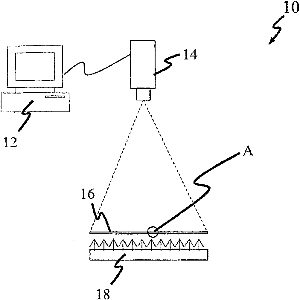
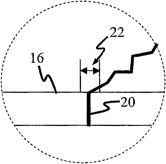
[0030] Referring to the accompanying drawings, embodiments of the invention described below relate to producing high contrast images of solar wafers for inspection purposes to facilitate detection of micro-cracks on solar wafers.
[0031] Conventional methods and systems for producing images of solar wafers do not produce images of high enough contrast to detect microscopic cracks in solar wafers. Furthermore, the increasing use of polycrystalline wafers for the manufacture of solar cells has increased the difficulty of detecting micro-cracks using the aforementioned conventional methods and systems.
[0032] For the sake of brevity and clarity, the following description of the invention will be limited to its application to improved systems and methods for facilitating the detection of microcracks in wafers used to fabricate solar cells. However, this is not intended to limit or exclude embodiments of the invention to other scopes of application that facilitate inspection of ...
PUM
 Abstract
Description
Claims
Application Information
 - R&D
- Intellectual Property
- Life Sciences
- Materials
- Tech Scout
- Unparalleled Data Quality
- Higher Quality Content
- 60% Fewer Hallucinations
Browse by: Latest US Patents, China's latest patents, Technical Efficacy Thesaurus, Application Domain, Technology Topic, Popular Technical Reports.
© 2025 PatSnap. All rights reserved.Legal|Privacy policy|Modern Slavery Act Transparency Statement|Sitemap|About US| Contact US: help@patsnap.com