Data processing method for testing parameters of chips

A parametric testing and data processing technology, applied in electronic circuit testing, single semiconductor device testing, etc., can solve the problem of prolonging the reading cycle, and achieve the effect of shortening the extraction cycle and speeding up the speed.

Inactive Publication Date: 2011-07-27
SHANGHAI INTEGRATED CIRCUIT RES & DEV CENT
View PDF5 Cites 22 Cited by
  • Summary
  • Abstract
  • Description
  • Claims
  • Application Information

AI Technical Summary

Problems solved by technology

[0004] The purpose of the present invention is to provide a data processing method for chip parameter testing to

Method used


Image

  • Data processing method for testing parameters of chips
  • Data processing method for testing parameters of chips
  • Data processing method for testing parameters of chips

Examples


Embodiment Construction

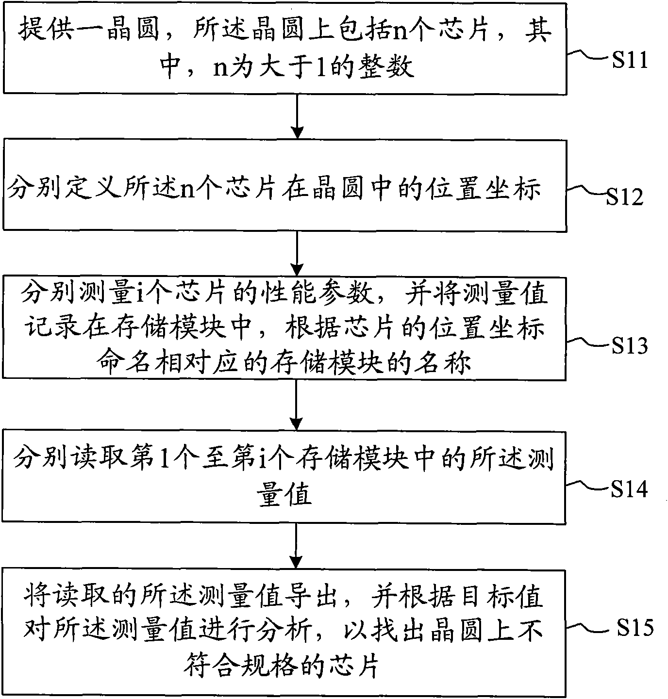
[0025] The present invention will be further described in detail below in conjunction with the accompanying drawings and specific embodiments. Advantages and features of the present invention will be apparent from the following description and claims. It should be noted that all the drawings are in very simplified form and use imprecise ratios, which are only used for the purpose of conveniently and clearly assisting in describing the embodiments of the present invention.
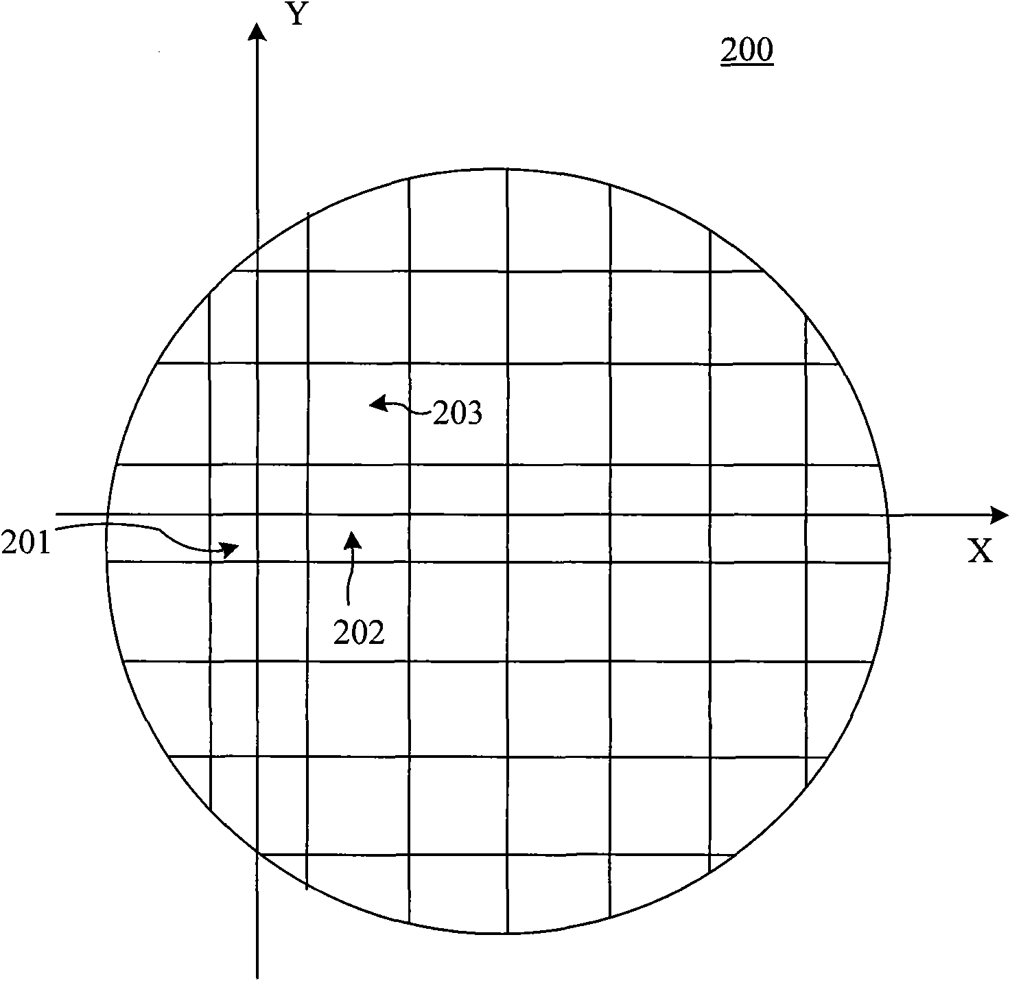
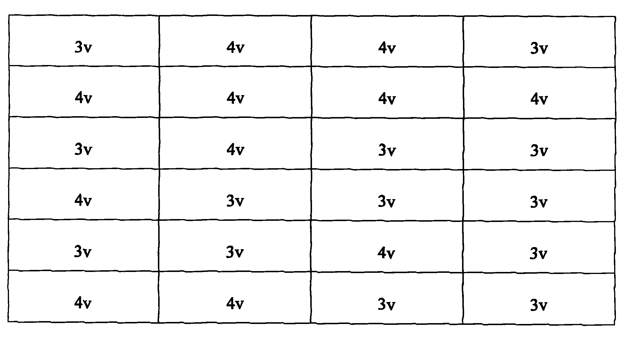
[0026] The core idea of ​​the present invention is to provide a data processing method for chip parameter testing. The method names the corresponding memory module according to the position coordinates of the chip, which is convenient for searching or reading the parameter measurement value of a chip at a certain position in the wafer. , the data processing method of the chip parameter test greatly shortens the extraction period of the chip parameter measurer, and accelerates the speed of chip development a...


PUM


Abstract

The invention provides a data processing method for testing parameters of chips, which comprises the following steps: providing a wafer, wherein the wafer comprises n chips, and n is an integer which is greater than 1; defining position coordinates of the n chips in the wafer respectively; measuring the performance parameters of i chips respectively, and recording measured values in memory modules, wherein i is the integer which is greater than 1, i is not more than n, each chip corresponds to one memory module, and names of the corresponding memory modules are named according to the position coordinates of the chips; reading the measured values from the first module to the ith memory module respectively; and exporting the read measured values, and analyzing the measured values according to a target value so as to find the chips which do not meet the specification on the wafer. By adopting the data processing method for testing the parameters of the chips, the extraction period of a chip parameter measurer can be greatly shortened, and the chip development speed and the process development speed can be accelerated.

Description

technical field [0001] The invention relates to the field of chip parameter information, in particular to a data processing method for chip parameter testing. Background technique [0002] In the manufacturing process of semiconductor components, the wafer process is an important basis for subsequent processes. The wafer manufacturing process is to manufacture electronic circuit components on a silicon wafer. After the fabrication is completed, a grid of dies is formed on the wafer, and then the wafer testing step conducts electrical tests on the dies, and disqualifies the unqualified dies. disuse. With the development of semiconductor technology, chips have entered the era of ultra-deep submicron and even nanometers, and various effects in devices have become more and more complex. Therefore, the compact model of chips has become larger and larger, and it is necessary to extract The number of parameters is also quite amazing. When adopting the traditional chip parameter ...

Claims


Application Information

Patent Timeline
IPC IPC(8): G01R31/28G01R31/26
Inventor 冯程程叶红波唐逸
Owner SHANGHAI INTEGRATED CIRCUIT RES & DEV CENT
Why Eureka
Try Eureka