P type microcrystalline silicon carbon film material for PI flexible substrate solar cell and preparation

A technology for solar cells and flexible substrates, applied in metal material coating processes, circuits, photovoltaic power generation, etc., can solve the problems of low conductivity, structural mismatch, low activation energy and light absorption, and achieve the effect of high conductivity

Inactive Publication Date: 2011-08-03
NANKAI UNIV
View PDF3 Cites 6 Cited by
  • Summary
  • Abstract
  • Description
  • Claims
  • Application Information

AI Technical Summary

Benefits of technology

This patented technology allows for control over how well the p type windows (P) layers have been structured or adjusted during manufacturing processes without affecting their electrical properties such as current flow through them. Additionally, this process helps create an excellent surface that can be used on both rigid and foldable materials like plastics while still maintaining its effectiveness at converting light into electricity.

Problems solved by technology

This patented technical problem addressed in this patents relates to finding ways to improve the performance of p type semiconductor films used for photovoltaic devices such as crystal Si or CdTe based on specific properties like narrower optically active bands at different wavelengths.

Method used


Image

  • P type microcrystalline silicon carbon film material for PI flexible substrate solar cell and preparation
  • P type microcrystalline silicon carbon film material for PI flexible substrate solar cell and preparation

Examples


Embodiment 1

[0039] On Eagle2000 glass substrate, adopt silane, hydrogen, borane, methane as reactive gas, by PECVD method, radio frequency power source frequency is 13.56MHz, according to the preparation method that thin film solar cell uses P-type window layer of the present invention to comprise Step, select the deposition parameters, where the reaction parameters are as follows:

[0040] Substrate temperature: 150°C,

[0041] Power density: 350mW / cm2,

[0042] Reaction pressure: 200Pa,

[0043] Silane concentration: 0.55%,

[0044] Borane doping concentration: 0.5%,

[0045] Methane doping concentration: 7.5%.

[0046] The prepared P-type microcrystalline silicon carbon material has a conductivity of 0.15 S / cm, a band gap greater than 2.0 eV, and a crystallization rate of 45.4% under the premise of a thickness of 30 nm.

Embodiment 2

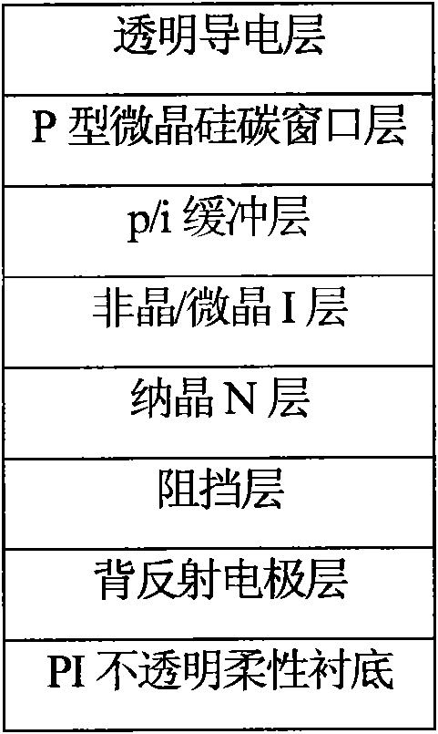
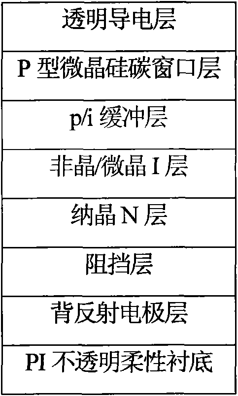
[0048] The substrate temperature is fixed at 150°C and the power density is 350mW / cm 2 .The silane concentration is 0.55%, the borane doping concentration is 0.5%, under the condition of keeping the total gas flow constant, the carbon-silicon ratio (CH 4 / SiH 4 ) varies between 7.5% and 13.75%, and the dark state conductivity σ can be obtained by adjusting the doping amount of methane d 0.15S / cm and optical bandgap E g The P-type microcrystalline silicon carbon material above 2.0eV, combined with the optimized carbon-doped p / i buffer layer for PI opaque flexible substrate thin film battery, obtained an open circuit voltage of 0.87V and a short circuit current density of 11.98mA / cm 2 , the fill factor is 54%, and the photoelectric conversion efficiency is 5.67%.

[0049] In summary, the P-type microcrystalline silicon carbon combines the advantages of the wide band gap of the P-type amorphous silicon carbon and the high conductivity and low light absorption of the P-type mic...


PUM

PropertyMeasurementUnit
Power densityaaaaaaaaaa
Conductivityaaaaaaaaaa
Bandgapaaaaaaaaaa

Abstract

The invention relates to a P type microcrystalline silicon carbon film material for a PI flexible substrate solar cell and preparation, belonging to the field of a film solar cell in new energy. The thickness of the P type microcrystalline silicon carbon film material layer is 15-30nm, the conductance is 0.15S/cm-10S/cm, the band gap is more than 2.0eV, and the crystallization rate is 30%-50%. By the optimization research for changing the proportion of carbon doping, the photoelectric performance and the structural characteristics of the material are controlled. P type microcrystalline silicon carbon with high conductance and wide band gap is obtained by utilizing the effect that carbon atom introduction can increase the band gap of a silicon film. The invention has the beneficial effects that the P type microcrystalline silicon carbon material with wide band gap is used in the PI non-transparent flexible substrate amorphous silicon film solar cell and is combined with an optimized p/i buffer layer, the built-in electric field of the film solar cell can be obviously strengthened, the open-circuit voltage of the cell is increased, and therefore the amorphous silicon film solar cell with high photoelectric conversion efficiency is obtained.

Description


Claims


Application Information

Patent Timeline
Owner NANKAI UNIV
Why Eureka
Try Eureka