Test package scan chain balancing method based on mean value allowance in SoC (System On Chip) test

A technology for testing packaging and scanning chains, which is applied in the direction of measuring devices, measuring electricity, and measuring electrical variables, etc. It can solve the problems that the global optimization guidelines are not close to the actual situation, and the BFD algorithm does not have global optimization.

Inactive Publication Date: 2011-08-17
HARBIN INST OF TECH
View PDF3 Cites 7 Cited by
  • Summary
  • Abstract
  • Description
  • Claims
  • Application Information

AI Technical Summary

Problems solved by technology

The disadvantage of this method is: BFD algorithm does not have the ability of global optimization
[0006] In addition, the above-mentioned Wrapper scan chain balance algorithm based on the average value to realize the SOC test method does not always give priority to the current ...

Method used


Image

  • Test package scan chain balancing method based on mean value allowance in SoC (System On Chip) test
  • Test package scan chain balancing method based on mean value allowance in SoC (System On Chip) test
  • Test package scan chain balancing method based on mean value allowance in SoC (System On Chip) test

Examples


specific Embodiment approach 1

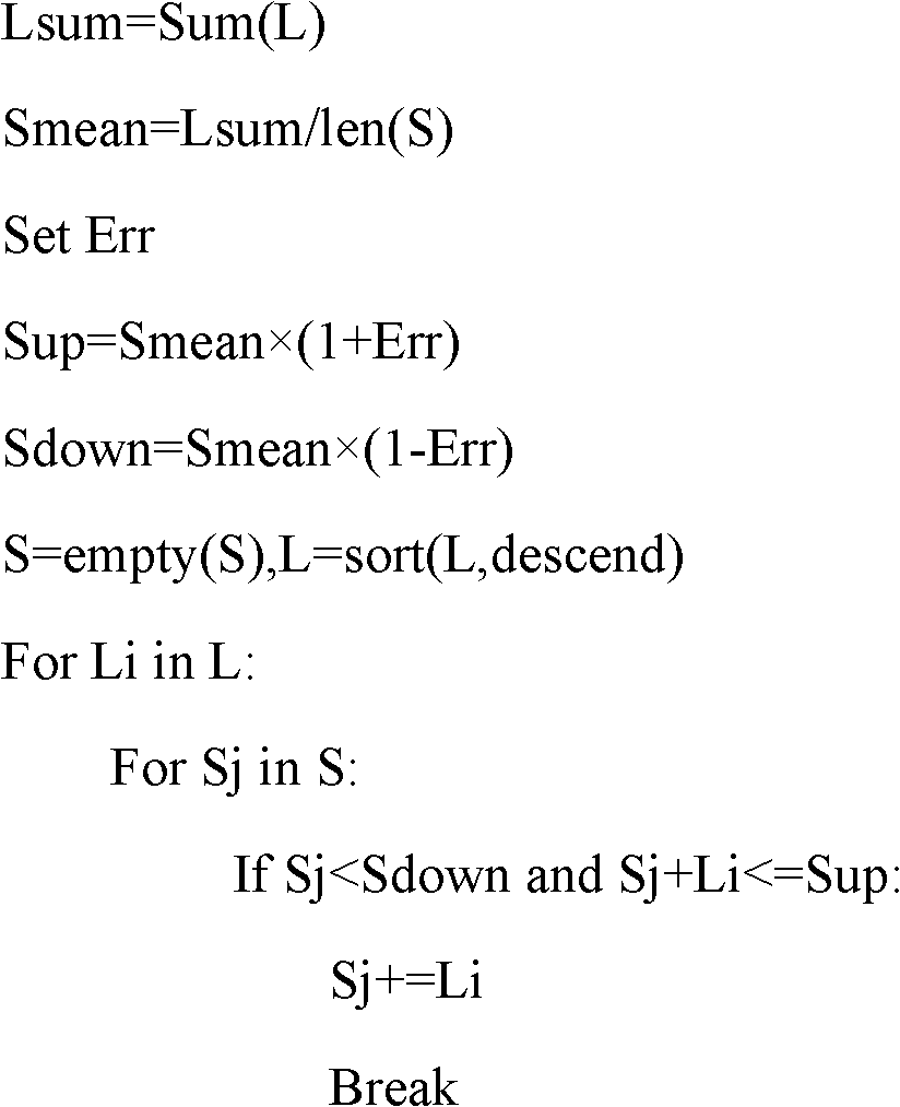
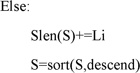
[0029] DETAILED DESCRIPTION OF THE PREFERRED EMBODIMENTS 1. The process of the method for balancing the scan chain of the test package scan chain based on the average margin in the SoC test described in this embodiment is:

[0030] First, calculate the average length of the Wrapper scan chain;

[0031] Then, an error limit is determined according to the obtained average length, and the error limit is 1% to 3% of the average length;

[0032] Finally, the value range is calculated according to the error limit and the average value of the Wrapper scan chain length, and the value range is used as a guiding principle for global optimization to realize the balance of the test package scan chain.

[0033] The scan chain balancing method described in this embodiment uses a range near the average value of the Wrapper scan chain length as a guiding principle for global optimization, making it closer to the actual situation, and this algorithm always prioritizes the current longest inter...


PUM


Abstract

The invention provides a test package scan chain balancing method based on a mean value allowance in a SoC (System On Chip) test, which relates to the technical field of system chip tests. The invention solves shortcomings in a traditional test package scan chain balancing method based on a BFD (Bidirectional Forwarding Detection) algorithm and a traditional SoC scan chain balancing method based on mean value approximation. The process of the test package scan chain balancing method comprises the following steps of: first, calculating a length mean value of a Wrapper scan chain; and then determining an error limit according to the obtained length mean value, wherein the error limit is 1-3% of the length mean value; and finally, calculating to obtain a value range according to the error limit and the length mean value of the Wrapper scan chain and balancing the test package scan chain by using the value range as a guiding principle of global optimization. In the invention, the target of reducing a testing time of a single IP (Internet Protocol) core is realized by using a Wrapper scan chain balancing algorithm so as to reduce the SoC testing time.

Description

technical field [0001] The invention relates to the technical field of system chip (SoC) testing. Background technique [0002] Introducing a "system-on-chip" (System-on-Chip, SoC) into engineering design can simplify design, shorten time-to-market, and increase system stability. However, as the scale of SoC increases, SoC testing gradually becomes the bottleneck in its manufacturing process, and the cost of SoC testing is also increasing. The SoC test time is an important factor affecting SoC test cost and efficiency. [0003] SoC testing usually includes three parts: Test Access Mechanism (TAM), Test Package (Wrapper), and Test Scheduling (Scheduling). The test access mechanism describes how the test port of the IP (Intellectual Property) core is accessed by the outside world. The test package is to add a layer of interface to the IP core to achieve a specific TAM. Finally, the test schedule describes the sequence of IP core tests. [0004] Literature Vikram Iyengar, Kr...

Claims


Application Information

Patent Timeline
IPC IPC(8): G01R31/3185
Inventor 俞洋彭宇杨智明陈叶富邓立宝彭喜元
Owner HARBIN INST OF TECH
Why Eureka
Try Eureka