Wafer support device and wafer processing process

A technology for supporting devices and wafer processing, applied in electrical components, semiconductor/solid-state device manufacturing, circuits, etc., can solve the problem that ultra-thin wafers cannot be tested in time, and achieve the effect of reducing process risks

Active Publication Date: 2011-08-17
SHANGHAI HUAHONG GRACE SEMICON MFG CORP
View PDF7 Cites 7 Cited by
  • Summary
  • Abstract
  • Description
  • Claims
  • Application Information

AI Technical Summary

Problems solved by technology

[0008] The purpose of the present invention is to provide a wafer supporting device and wafer processing technology to solve the problem that the existing ultra-thin wafers cannot be tested in time

Method used


Image

  • Wafer support device and wafer processing process
  • Wafer support device and wafer processing process
  • Wafer support device and wafer processing process

Examples


Embodiment Construction

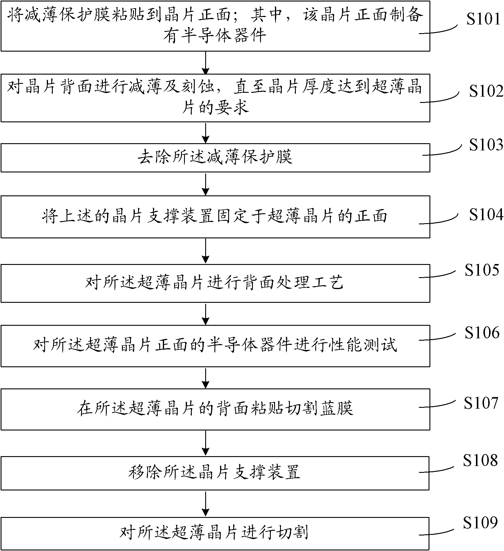
[0034] The wafer supporting device and wafer processing technology proposed by the present invention will be further described in detail below in conjunction with the accompanying drawings and specific embodiments. Advantages and features of the present invention will be apparent from the following description and claims. It should be noted that the drawings are all in a very simplified form and use imprecise ratios, which are only used to facilitate and clearly assist the purpose of illustrating the embodiments of the present invention.
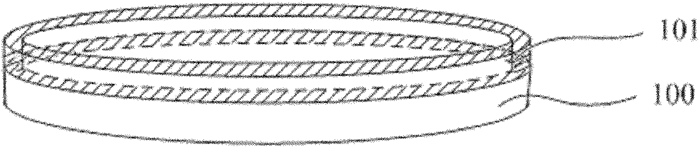
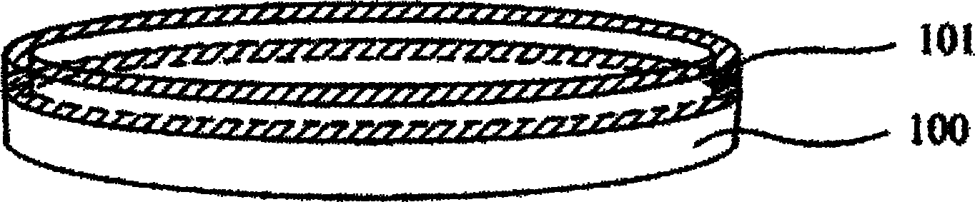
[0035] The core idea of ​​the present invention is to provide a wafer supporting device, which is in the form of a circular cylindrical structure, so that it will not block the semiconductor device area on the front of the ultra-thin wafer, so performance testing can be performed in time before packaging, and feedback and evaluation can be performed in time The problem in the process reduces the risk of the process; at the same time, it also...


PUM


Abstract

The invention discloses a wafer support device. The device has an annular cylindrical structure so that a semiconductor device area on the front surface of an ultra-thin wafer cannot be blocked. Therefore, a performance test can be performed before encapsulating; problems in a process can be fed back and evaluated timely; and process risks are reduced. The invention also discloses a wafer processing process. In the processing process, the wafer support device is utilized for supporting the ultra-thin wafer in the process of a wafer back surface processing process and the performance test is performed after the wafer back surface processing, so that the problems in the process can be fed back and evaluated timely, and the process risks are reduced.

Description

technical field [0001] The invention relates to the technical field of integrated circuits, in particular to a wafer supporting device and a wafer processing technology. Background technique [0002] With the advancement of integrated circuit technology, semiconductor integrated circuits are developing in the direction of thinner and smaller while the degree of integration, speed and reliability are continuously improved. And with the introduction of through-silicon via (TSV, Through Silicon Via) 3D packaging technology, the requirements for chip thickness are getting higher and higher, and ultra-thin chips have emerged as the times require. The so-called ultra-thin wafer refers to a wafer whose thickness is equal to or less than 100um. At the same time, because ultra-thin wafers have low resistance, low power dissipation and good thermal conductivity, they have also become the focus of research in power electronic devices. [0003] Ultra-thin wafers are usually realized t...

Claims


Application Information

Patent Timeline
Patent Type & Authority Applications(China)
IPC IPC(8): H01L21/683H01L21/00
Inventor 刘玮荪傅荣颢
Owner SHANGHAI HUAHONG GRACE SEMICON MFG CORP
Why Eureka
Try Eureka