Single-substrate multi-chipset high-power LED (Light-Emitting Diode) encapsulation one-step bonding method

A LED packaging and multi-chip technology, applied in electrical components, electrical solid devices, circuits, etc., can solve problems such as long bonding time, achieve the effects of improved packaging efficiency, efficient thermal management, and reduced costs

Inactive Publication Date: 2011-08-17
HARBIN INST OF TECH
View PDF5 Cites 13 Cited by
  • Summary
  • Abstract
  • Description
  • Claims
  • Application Information

AI Technical Summary

Problems solved by technology

[0005] The purpose of the present invention is to solve the problem that in the existing multi-chipset high-power LED packaging technology, the bonding of multiple chips is carried out sequentially, resulting in too long overall bonding time, and to provide a single-substrate multi-chipset high-power LED packaging once Bonding method

Method used


Image

  • Single-substrate multi-chipset high-power LED (Light-Emitting Diode) encapsulation one-step bonding method
  • Single-substrate multi-chipset high-power LED (Light-Emitting Diode) encapsulation one-step bonding method
  • Single-substrate multi-chipset high-power LED (Light-Emitting Diode) encapsulation one-step bonding method

Examples


specific Embodiment approach 1

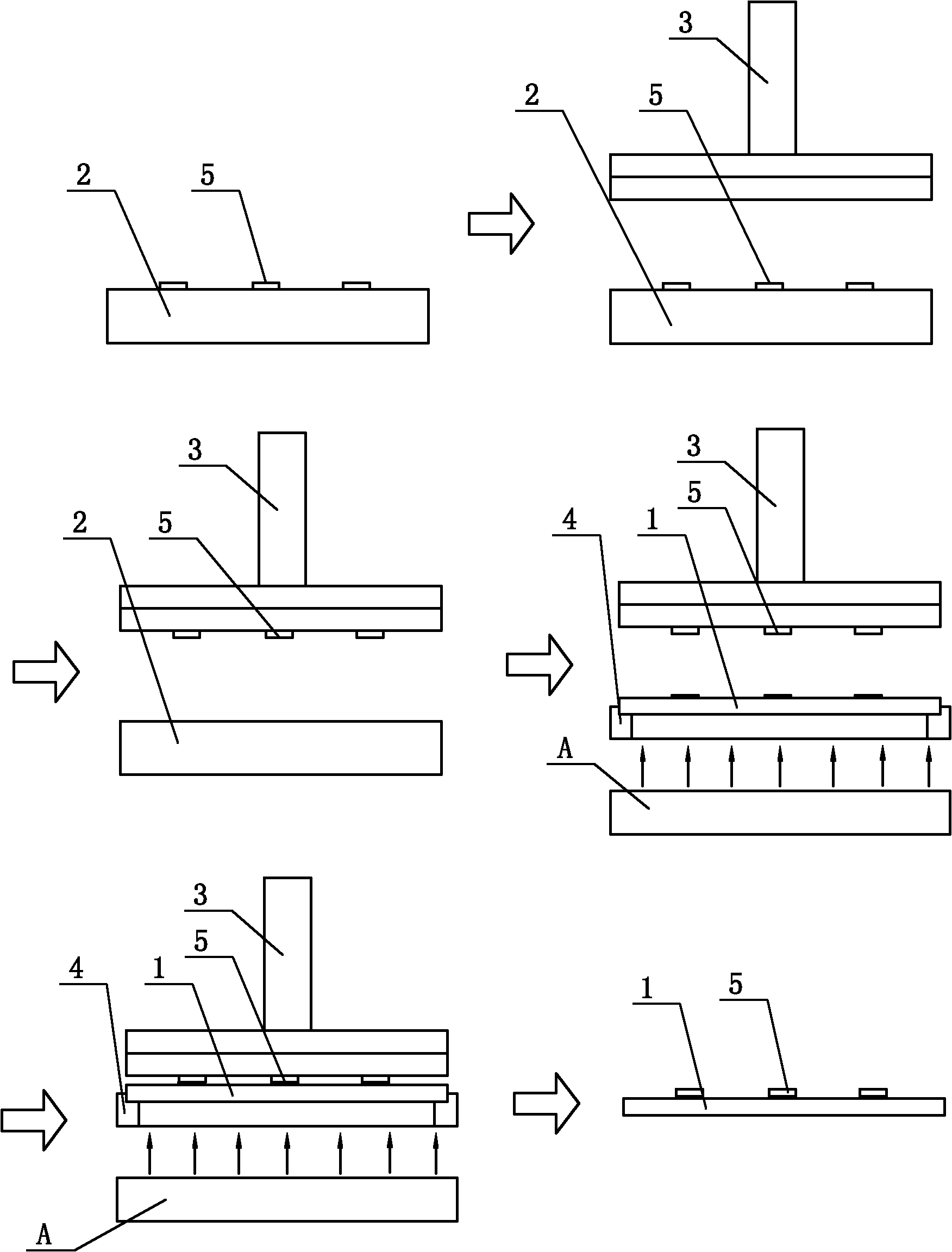
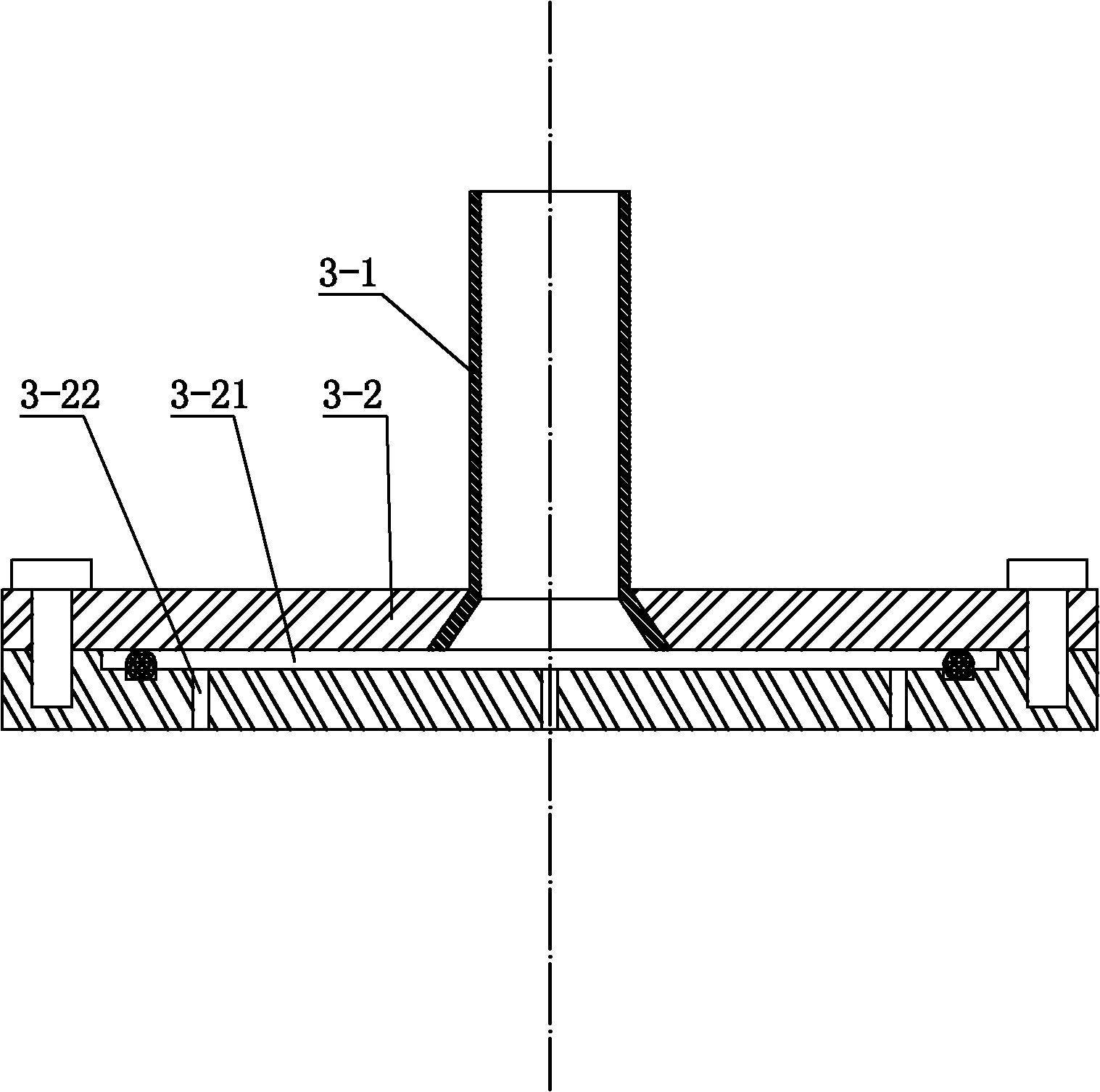
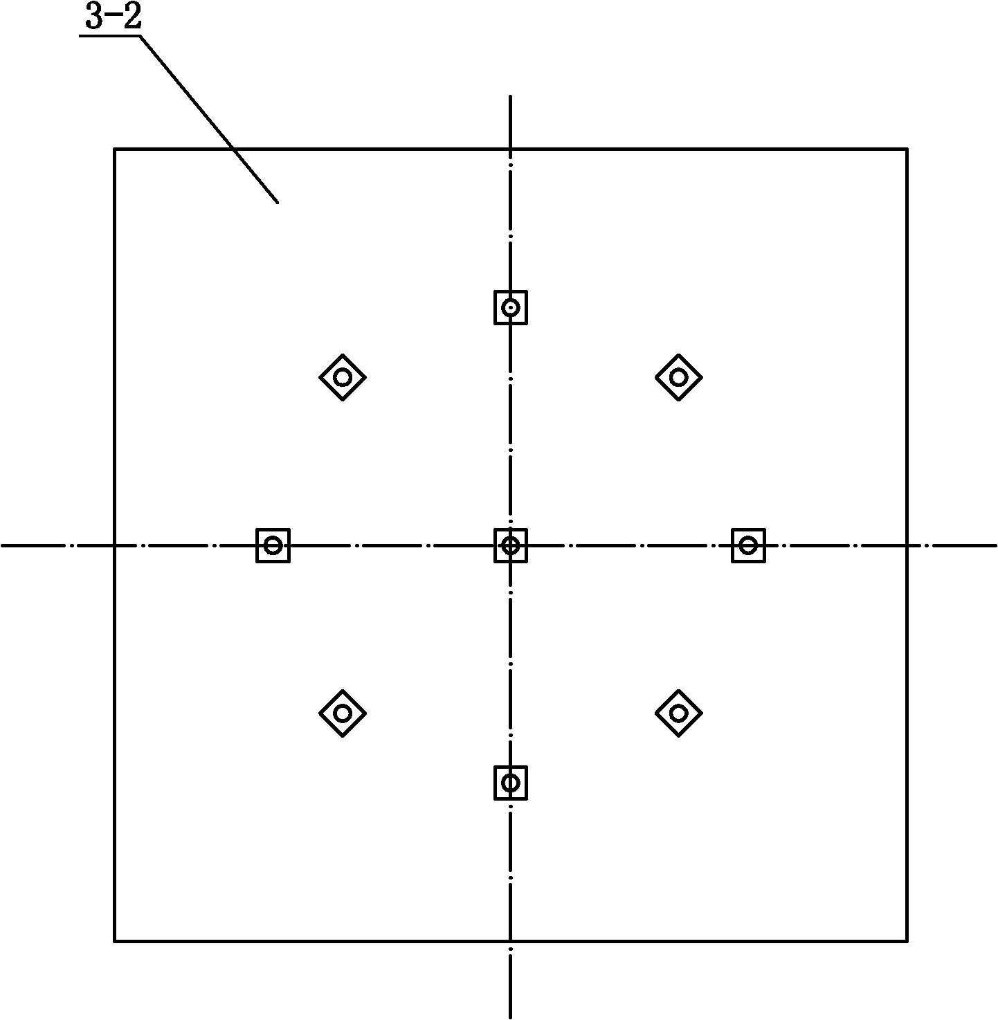
[0019] Specific implementation mode one: the following combination Figure 1 to Figure 6 Describe this implementation mode, this implementation mode comprises the following steps:

[0020] Step 1: cleaning the substrate 1, the slide table 2, the multi-chip nozzle 3 and the support table 4;

[0021] Step 2: Place the substrate 1 on the support table 4; determine the position of the chip to be bonded on the front of the substrate 1, and place a plurality of chips 5 to be bonded on the carrier according to the arrangement corresponding to the position of the chip to be bonded on stage 2;

[0022] Step 3: uniformly apply the solder paste on the positions of the chips to be bonded by screen printing, and then use the multi-chip suction nozzle 3 to simultaneously pick up multiple chips 5 to be bonded;

[0023] Step 4: Use a heat source to heat the back of the substrate 1, align the multiple chips 5 to be bonded picked up by the multi-chip suction nozzle 3 to the position to be bon...

specific Embodiment approach 2

[0026] Embodiment 2: This embodiment is a further description of Embodiment 1, and the cleaning is ultrasonic cleaning. Other components and connections are the same as those in Embodiment 1.

specific Embodiment approach 3

[0027] Embodiment 3: This embodiment is a further description of Embodiment 1, and the solder paste is eutectic alloy solder paste. Other components and connections are the same as those in Embodiment 1.

[0028] The thermal conductivity of the eutectic alloy solder paste is much greater than that of the conductive adhesive and thermal conductive adhesive, which is more conducive to the heat dissipation of the package structure.


PUM


Abstract

The invention relates to a single-substrate multi-chipset high-power LED (Light-Emitting Diode) encapsulation one-step bonding method, belonging to the technical field of multi-chipset high-power LED encapsulation. The invention solves the problem that the whole bonding time is too long as multiple chipsets are sequentially spliced in the traditional multi-chipset high-power LED encapsulation technology. The method comprises the following steps of: cleaning a substrate, a chip carrying platform, a multi-chip suction nozzle and a supporting platform; placing the substrate on the supporting platform; determining positions of chips to be bonded on the front of the substrate, and placing multiple chips to be bonded on the chip carrying platform corresponding to the positions of the chips to be bonded; uniformly coating soldering paste on the positions of the chips to be bonded by adopting screen printing, and then simultaneously picking up multiple chips to be bonded with the multi-chip suction nozzle; heating the back of the substrate, enabling multiple chips to align with the positions to be bonded and then attached to the soldering paste, continuously heating for 5-10s, naturally cooling to room temperature, and removing the multi-chip suction nozzle, thus the bonding process is completed. The invention provides an encapsulation bonding method.

Description

technical field [0001] The invention relates to a single-substrate multi-chip group high-power LED packaging one-time bonding method, which belongs to the technical field of multi-chip group high-power LED packaging. Background technique [0002] With the continuous progress of the national semiconductor lighting project and the constant call for energy conservation and emission reduction and low-carbon economy, LED lighting has received more and more attention. Compared with traditional incandescent lamps, under the same brightness, LED consumes only one-eighth of the electric energy of incandescent lamps. The application of LED lighting technology greatly saves energy, reduces carbon dioxide emissions, and effectively protects the global environment. High-power LEDs have good application prospects due to their advantages of long life, high luminous efficiency, and energy saving. The greater the power of the LED chip, the more heat it will generate during operation, which...

Claims


Application Information

Patent Timeline
Patent Type & Authority Applications(China)
IPC IPC(8): H01L33/00H01L33/48H01L33/64H01L25/075
Inventor 王春青杭春进
Owner HARBIN INST OF TECH
Why Eureka
Try Eureka