
Method for measuring micro-tube density in SiC (silicon carbide) crystal

A technology of crystals and micropipes, which is applied in the field of measuring the density of micropipes in SiC crystals, and can solve the problems of not being able to measure the measured area at one time

Inactive Publication Date: 2011-09-07
SHANDONG UNIV
View PDF1 Cites 3 Cited by
  • Summary
  • Abstract
  • Description
  • Claims
  • Application Information

AI Technical Summary

Problems solved by technology

However, the observation of this microtubules must rely on a microscope to complete, so the entire measured area cannot be measured at one time

Method used


Image

  • Method for measuring micro-tube density in SiC (silicon carbide) crystal
  • Method for measuring micro-tube density in SiC (silicon carbide) crystal
  • Method for measuring micro-tube density in SiC (silicon carbide) crystal

Examples


Embodiment 1

[0027] Example 1: Micropipe measurement was performed on a 4H-SiC wafer with a wafer diameter of 50.8 mm.

[0028] The microscope is a microscope from Japan OLYMPUS Company, with a magnification of 50 times, and the field of view is calibrated with a ruler, and the field of view under 50 times is 15.6mm 2 .

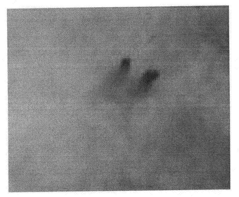
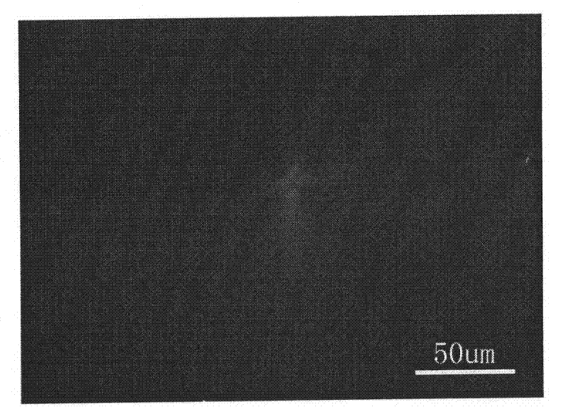
[0029] Microtubule distribution as Figure 4 As shown, according to the total number of micropipes on the obtained wafer area is 123 (the number of micropipes in the blank area is zero), then:

[0030]

Embodiment 2

[0031] Example 2: Micropipe measurement was performed on a 6H-SiC wafer with a wafer diameter of 75.6 mm. The microscope is a microscope from Japan OLYMPUS Company, with a magnification of 50 times, and the field of view is calibrated with a ruler, and the field of view under 50 times is 15.6mm 2 .

[0032] Microtubule distribution as Figure 6 As shown, according to the total number of micropipes on the obtained wafer area is 142 (the number of micropipes in the blank area is zero), then:

[0033]


PUM

PropertyMeasurementUnit
Diameteraaaaaaaaaa

Abstract

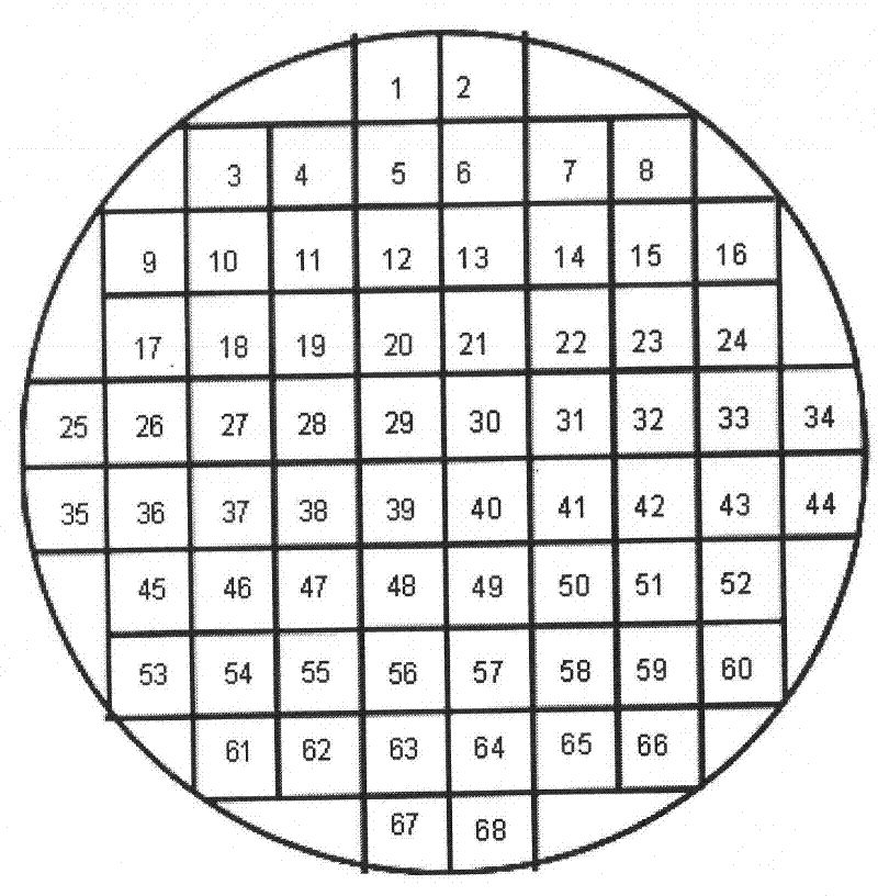
The invention relates to a method for measuring micro-tube density in a SiC (silicon carbide) crystal, which comprises the following steps: dividing a measured surface of the SiC crystal into a plurality of square regions and numbering the regions, wherein the area of each region is 5*5 square millimeters; taking a central point of each region as a measuring point, and microscopically measuring and recording the number of micro-tube in each viewing area, thereby acquiring the micro-tube density of the measured region, wherein the micro-tube density is equal to the number of micro-tube dividing the viewing area; and summing the number of micro-tube in all measured regions and acquiring the total number of the micro-tube on the measured surface of the SiC crystal within the viewing area, thereby acquiring the micro-tube density in the whole SiC crystal. Without using the scheme of synchronous radiation light source or corrosion, the method provided by the invention can be used for measuring by using a microscope and has the advantages of all-crystal observation, non-contact and non-destruction.

Description

technical field [0001] The invention provides a method for measuring the density of micropipes in SiC crystals, belonging to the technical field of crystal measurement. Background technique [0002] SiC is a representative of the third-generation wide-bandgap semiconductor, which has excellent electrical and thermal properties such as large bandgap, high mobility, and high thermal conductivity. It can be used in extreme situations such as high temperature, high pressure, and strong radiation, and is an ideal semiconductor for high-power solid-state devices. [0003] The main factor affecting the application of silicon carbide at present is its high density of defects. The most common defects in silicon carbide bulk crystals are called micropipes. Microtubules are hollow super screw dislocations with their Burgers vector along the C axis. A number of causes have been proposed or identified for the generation of microtubules. These reasons include Si or C inclusions, bound...

Claims


Application Information

Patent Timeline
IPC IPC(8): G01N9/00
Inventor 王翎彭燕徐现刚胡小波宁丽娜
Owner SHANDONG UNIV
Learn More