Liquid crystal display device

A liquid crystal display device and liquid crystal technology, applied in nonlinear optics, instruments, optics, etc., can solve the problems of complex manufacturing process and slow response

Inactive Publication Date: 2011-09-14
SHARP KK
View PDF2 Cites 23 Cited by
  • Summary
  • Abstract
  • Description
  • Claims
  • Application Information

AI Technical Summary

Problems solved by technology

However, the MVA mode not only has a complicated manufacturing process, but a

Method used


Image

  • Liquid crystal display device
  • Liquid crystal display device
  • Liquid crystal display device

Examples


Embodiment approach 1

[0089] The liquid crystal display device of this embodiment is a liquid crystal display device using a transverse electric field method called a TBA method. In this transverse electric field method, an electric field (transverse electric field) in the direction of the substrate surface is applied to the liquid crystal layer to control the orientation of the liquid crystal molecules. Image display.

[0090] figure 1 It is a schematic plan view showing the configuration of the liquid crystal display device of Embodiment 1. FIG. In addition, although only one or two picture elements are shown in the following figures, a plurality of picture elements (sub-pixels) are provided in a matrix in the display area (image display area) of the liquid crystal display device of this embodiment.

[0091] The liquid crystal display device of the present embodiment includes a liquid crystal display panel having a pair of oppositely arranged substrates, namely, an active matrix substrate (TFT ...

Embodiment approach 2

[0217] Figure 25 It is a schematic plan view showing the configuration of a liquid crystal display device according to Embodiment 2. FIG.

[0218] The liquid crystal display device of this embodiment has the same configuration as that of the first embodiment except for the layout of the pixel electrodes and the common electrodes, so only the differences from the first embodiment will be described in detail.

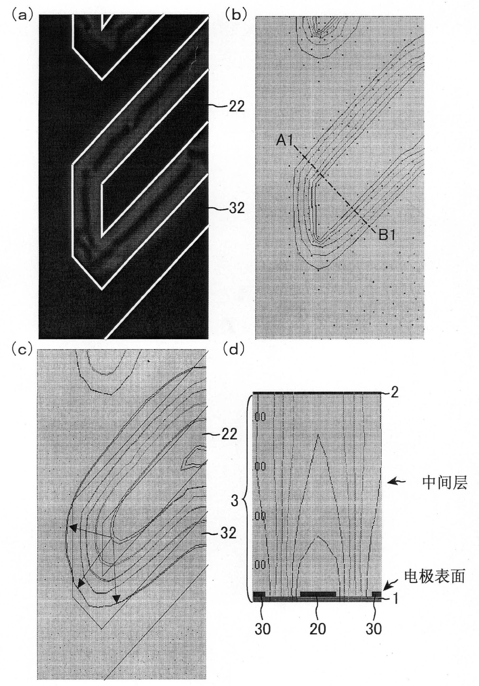
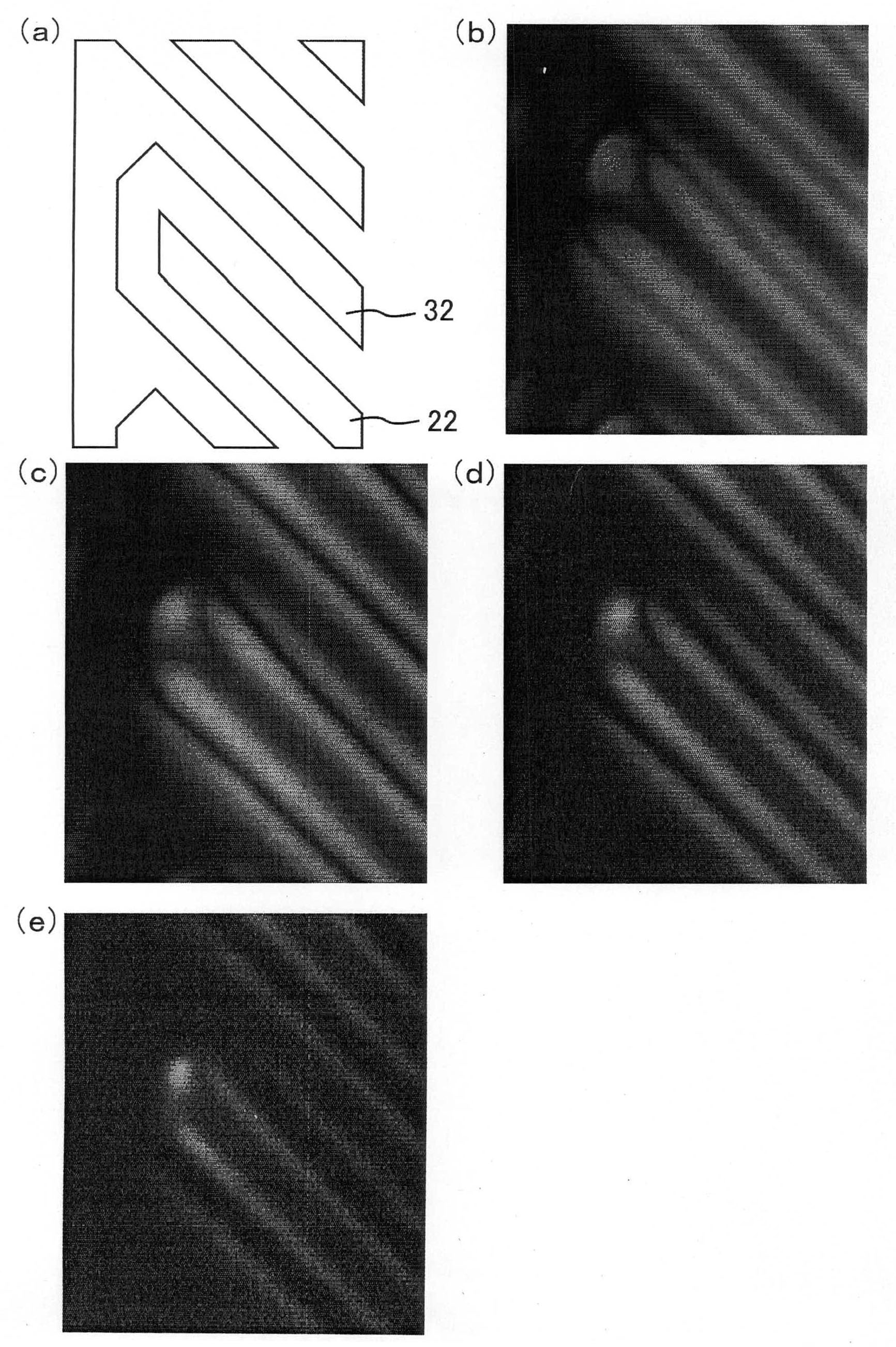
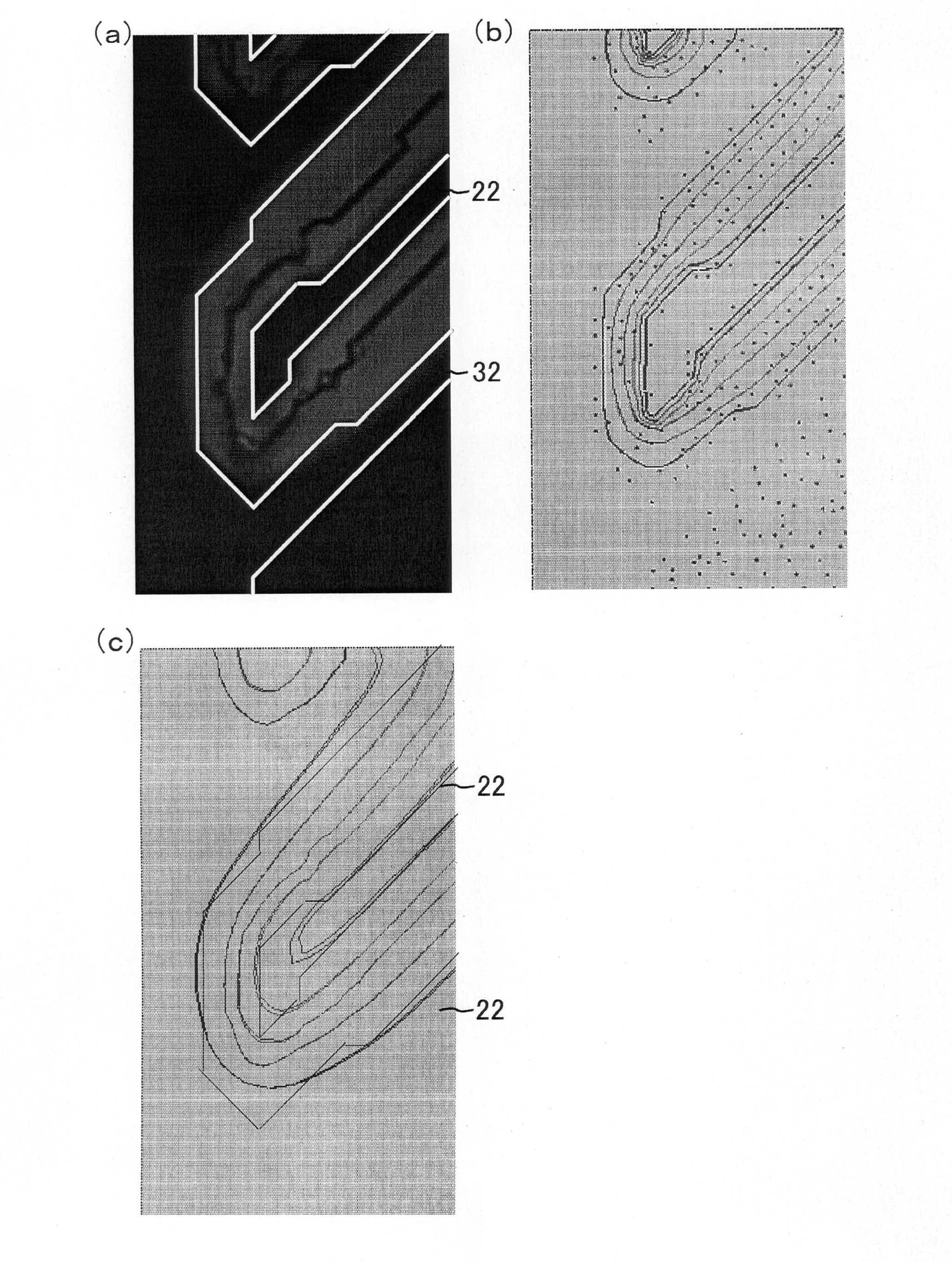
[0219] The liquid crystal display device of this comparative method such as Figure 25 As shown, it includes: a comb-shaped pixel electrode 220 having a trunk portion 221 and branches 222 ; and a comb-shaped common electrode 230 having a trunk portion 231 and branches 232 . In addition, the gaps between the electrodes in the area surrounding the branch portion 222 or the branch portion 232 are not chamfered, and the electrode intervals in this area are not evenly spaced.

[0220] Figure 26 It is a figure which shows the simulation result of the liquid crystal display...

Embodiment approach 3

[0224] The liquid crystal display device of Embodiment 3 has the same configuration as that of the liquid crystal display device of Embodiment 2 except that L / S=4.0 μm / 12.0 μm is set.

[0225] (comparison method 2)

[0226] The liquid crystal display device of Comparative Embodiment 2 has the same configuration as the liquid crystal display device of Embodiment 2 except that L / S=2.5 μm / 7.5 μm is set.

[0227] (comparison method 3)

[0228] The liquid crystal display device of Comparative Embodiment 3 has the same configuration as the liquid crystal display device of Embodiment 2 except that L / S=2.5 μm / 5.0 μm is set.

[0229] (comparison method 4)

[0230] The liquid crystal display device of Comparative Embodiment 4 has the same configuration as the liquid crystal display device of Embodiment 2 except that L / S=2.5 μm / 4.0 μm is set.

[0231] (comparison mode 5)

[0232] The liquid crystal display device of Comparative Embodiment 5 has the same configuration as the liquid cr...


PUM


Abstract

Provided is a liquid crystal display device capable of preventing the occurrence of a residual image. The liquid crystal display device is provided with a first substrate and a second substrate which are disposed to face each other, and a liquid crystal layer sandwiched between the first substrate and the second substrate. The first substrate comprises a comb-shaped first electrode including first branch portions and a comb-shaped second electrode including second branch portions, and the first electrode and the second electrode are disposed to planarly face each other in a pixel. The liquid crystal layer includes p-type nematic liquid crystal and is driven by an electric field generated between the first electrode and the second electrode. The p-type nematic liquid crystal is aligned perpendicularly to the first substrate and the second substrate when no voltage is applied. The first branch portions and the second branch portions extend diagonally to boundaries between adjacent pixels, and the intervals between the first electrode and the second electrode in a region surrounding the tip of the first branch portion are substantially equal.

Description

technical field [0001] The present invention relates to a liquid crystal display device. More specifically, it relates to a display device suitable for a liquid crystal display device in a transverse bend alignment (TBA:Transverse Bend Alignment) mode. Background technique [0002] Liquid crystal display devices are characterized by thinness, light weight, and low power consumption, and are widely used in various fields. Moreover, its display performance has continued to improve significantly over time, to the point where it is now superior to a CRT (cathode ray tube). [0003] The display method of a liquid crystal display device is determined by how liquid crystals are arranged in a unit (unit cell). Conventionally, TN (Twisted Nematic: Twisted Nematic) mode, MVA (Multi-domain Vertical Alignment: Multi-domain Vertical Alignment) mode, and IPS (In-plane Switching: in-plane switching) are known as display methods of liquid crystal display devices. mode, OCB (Optically sel...

Claims


Application Information

Patent Timeline
IPC IPC(8): G02F1/1343
CPCG02F2001/133742G02F2001/13706G02F1/134363G02F1/133742G02F1/13706
Inventor 森下克彦松本俊宽冈崎敢
Owner SHARP KK
Why Eureka
Try Eureka