Imaging equipment

A camera device and image output technology, applied in image communication, exposure control, television and other directions, can solve problems such as jitter, afterimage, and image quality deterioration, and achieve the effect of preventing flickering

Inactive Publication Date: 2011-09-21
HITACHI LTD
View PDF6 Cites 16 Cited by
  • Summary
  • Abstract
  • Description
  • Claims
  • Application Information

AI Technical Summary

Problems solved by technology

In the captured images, many scenes contain illumination light from light sources such as fluorescent lamps and LED lighting. The flickering caused by the lighting cycle of the illumination light may cause the image to lose useful information or cause the quality of the image to deteriorate. Therefore, it is necessary to Perform flicker removal processing
[0019] As a method for solving the flicker of the monitoring camera, Patent Document 1 and Patent Document 2 disclose that the shutter is set to a predetermined number of times in each camera cycle to perform exposure control, so that the flicker can be reduced or eliminated. At the same time, there is a method of adjusting the exposure through the shutter, but since multiple exposures are performed in each camera cycle as a transmission and reception and the respective exposures are added, compared with the usual shutter speed control, there is a problem with the subject in motion. Problems such as afterimages and jitters occur

Method used


Image

  • Imaging equipment
  • Imaging equipment
  • Imaging equipment

Examples


Embodiment Construction

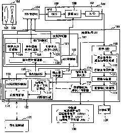
[0074] based on the following image 3 Embodiments of the imaging device of the present invention will be described.

[0075] A. Basic structure of camera system

[0076] (1) Explanation of the camera system

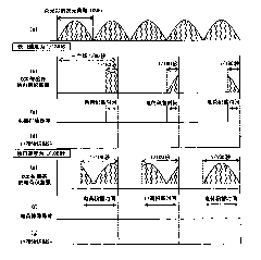
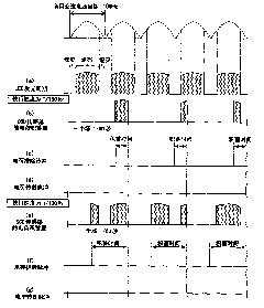
[0077] image 3 It is a block diagram showing an outline of an imaging device according to an embodiment of the present invention, wherein the imaging device has a fixed-aperture camera, and a control circuit built in the fixed-aperture camera has a flicker removal function.

[0078] First, the operation during shooting and recording and the flow of signals will be described. The captured image passes through the aperture 102 for adjusting the amount of external light obtained from the lens 101 in the lens unit 103 in the figure, and then is irradiated into the CCD sensor 104 having the imaging elements of the vertical transfer CCD and the horizontal transfer CCD, After photoelectric conversion, the image signal is input to an AFE circuit (Analog Front End Circuit, h...


PUM


Abstract

The present invention provides an imaging equipment. In an aperture fiation type imaging equipment, the problem is that: an image flicker is generated by a fluorescent lamp lighted in dependence on a commercial AC supply and a LED lighting, it is imposible to fix a shutter at the shutter speed at which the image flicker does not occur. Because each image in the imaging equipment for monitoring is very important information, it is necessary to still obtain the image in which a residual image or flicker is not present relative to to a moving imaging target even though the shutter speed is set at high speed. When a decision is made that the flicker is present, the timings of applying a discharging pulse and a charge readout pulse respectively are varied depending on a field in order to implement shutter speed control in a CCD sensor, so that the imaging equipment can be exposed to a portion of light falling into the same phase thereof within a luminescence period of the lighting during each field. After the start of the control, the phase point treatment is immediately performed, so that the timing of the exposure if the imaging equipment in the lighting period of lighting is set to ensure the part with maximum exposure amount to be exposed. Even though a light source emits light while being repeatedly lit and extinguished in a certain period, the exposure without flicker is performed.

Description

technical field [0001] The present invention relates to an imaging device capable of eliminating flicker of a periodic light source and a control method thereof. Background technique [0002] As an imaging element that converts an optical image into an electrical signal, for example, a solid-state imaging element such as a CCD sensor has been widely used in camera products such as consumer products and surveillance products. These camera products perform exposure control through aperture control, shutter speed control of an imaging element using an electronic shutter, automatic gain control (AGC, Automatic Gain Control), and ND filter, etc. Automatic exposure control (Auto Exposure Control, hereinafter referred to as "AE"), in order to obtain a certain amount of exposure. When a CCD sensor is used as an imaging element, the charge accumulation amount is controlled. [0003] The above-mentioned AE uses a program AE that determines which of the above-mentioned aperture contr...

Claims


Application Information

Patent Timeline
Patent Type & Authority Applications(China)
IPC IPC(8): H04N5/235G03B7/097
CPCH04N5/2351H04N5/353G03B7/093H04N5/2357H04N5/3728H04N23/745H04N23/71H04N25/53H04N25/73
Inventor 宫原宏幸安藤辉
Owner HITACHI LTD
Why Eureka
Try Eureka