Device packaging structure and packaging method thereof

A technology of device packaging and packaging methods, which is applied in the direction of electric solid-state devices, semiconductor devices, semiconductor/solid-state device manufacturing, etc., can solve the problems of poor heat dissipation performance, polluting the environment, consuming materials, and large heat dissipation area, etc., to achieve the goal of increasing the effective heat dissipation area Effect

Active Publication Date: 2013-07-17
济南市半导体元件实验所
View PDF6 Cites 0 Cited by
  • Summary
  • Abstract
  • Description
  • Claims
  • Application Information

AI Technical Summary

Problems solved by technology

[0011] Therefore, in order to overcome the structural characteristics of the current device packaging structure that make related devices have poor heat dissipation performance during use, pollute the environment, and consume a lot of materials, the present invention provides a device that can effectively dissipate heat with a large area and will not pollute the environment during use. and a device packaging structure that consumes less material. At the same time, in response to the device packaging structure, the present invention also provides a packaging method

Method used


Image

  • Device packaging structure and packaging method thereof
  • Device packaging structure and packaging method thereof
  • Device packaging structure and packaging method thereof

Examples


Embodiment Construction

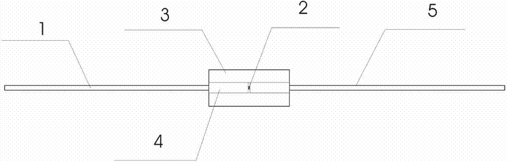
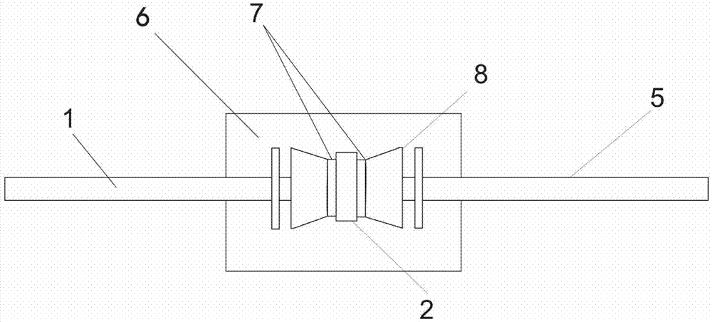
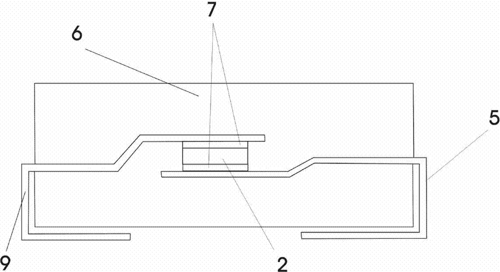
[0039] According to the present invention, a device packaging structure includes a package body and a chip 2 encapsulated in the package body, and a pair of leads 1 connected to the chip 2 and extending out of the package body, the package body having a cylindrical structure , The lead 1 is drawn from the bottom surface of the cylindrical structure, one for each of the two bottoms; the device packaging structure also includes a metal shell 10 correspondingly arranged at both ends of the package body, and the metal shell is electrically connected to the corresponding terminal lead, and It is electrically insulated from the different side metal shell and the different side leads.

[0040] Regarding the metal shell 10, it is nominally used for electrical connection, that is, the connection conversion is realized through the connection with the lead. At the same time, the metal can be related to the connection between itself and the package body, and can have a specific structure acc...


PUM


Abstract

The invention discloses a device packaging structure which has a large effective heat dissipation area and does not generate environmental pollution and consumes less materials. Besides, the invention also discloses a packaging method corresponding to the device packaging structure. According to the invention, the packaging structure comprises a package body, a wafer packaged in the package body, and a pair of leads connected with the wafer and extending out of the package body, the package body is of a cylindrical structure, the leads are led out from the two bottoms of the cylindrical structure respectively; the device packaging structure also comprises a metal shell respectively and correspondingly arranged at two ends of the package body, the connection area is large, the metal shell is electrically connected with the lead at the corresponding end, and is electrically insulated from the metal shell and the lead which are arranged at the opposite side. Based on the structure, the repair and welding of a pin is not necessary when in use, material consumption is small and additional pollution cannot be generated.

Description

Technical field [0001] The invention relates to a device packaging structure, which belongs to the packaging structure of electronic devices used in circuit boards; at the same time, the invention also provides a packaging method of the device packaging structure. Background technique [0002] In the development process of electronic devices, many packaging forms have been produced in response to different technological levels and different objective needs in different periods. At present, electronic devices can be divided into plug-in and surface-mount categories in terms of packaging, but the common feature is that they are connected to the circuit board through leads, pass current through the leads, and use the metal material characteristics of the leads to enhance part of the heat dissipation capacity. The increase in heat dissipation capacity depends on the thermal conductivity of the lead material, the heat capacity of the lead body and the heat dissipation area of ​​the le...

Claims


Application Information

Patent Timeline
Patent Type & Authority Patents(China)
IPC IPC(8): H01L23/31H01L23/48H01L23/367H01L21/56H01L21/60
CPCH01L24/01
Inventor 张洪亮季群邢腾刘博
Owner 济南市半导体元件实验所
Why Eureka
Try Eureka