Solid-state imaging device

A solid-state imaging device and unit pixel technology, which is applied in the direction of electric solid-state devices, semiconductor devices, electrical components, etc., can solve the problems that signal charges cannot be read out and are insufficient

Inactive Publication Date: 2011-09-28
KK TOSHIBA
View PDF5 Cites 9 Cited by
  • Summary
  • Abstract
  • Description
  • Claims
  • Application Information

AI Technical Summary

Problems solved by technology

With the reduction of the pixel size, there is a problem that the charge storage capacity of the FD (dynamic range: dynamic range ) is insufficient, and all the signal charges after conversion and storage of the photodiode cannot be read out to the FD.

Method used


Image

  • Solid-state imaging device
  • Solid-state imaging device
  • Solid-state imaging device

Examples


Embodiment Construction

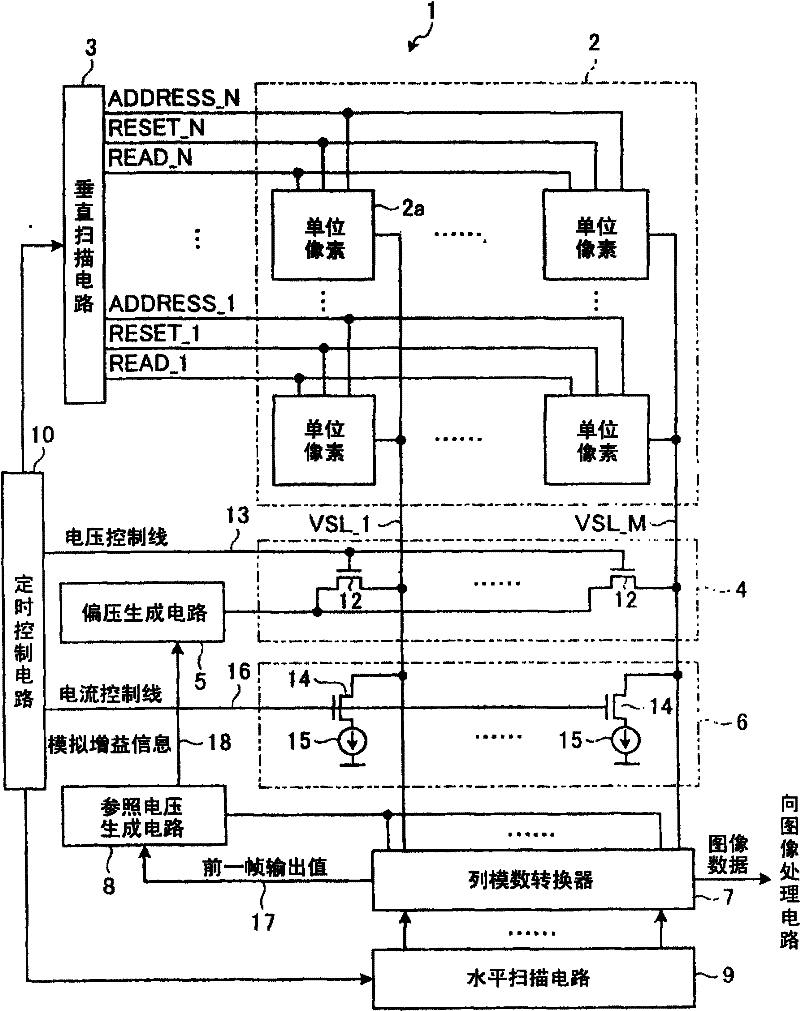
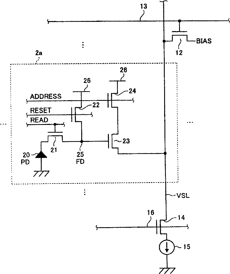
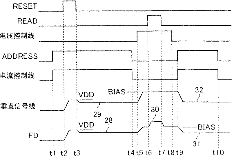
[0018] According to the present embodiment, the pixel drive circuit that uniformly controls the drive of each unit pixel in one row of the pixel array does not apply a bias voltage from the bias voltage generating circuit to the vertical signal line, and configures the amplifying transistor as a source tracker circuit. The reset transistor is turned on, and the floating diffusion layer is connected to the power supply. A pixel signal (reset voltage) is output from the floating diffusion layer to the vertical signal line. Then, the above-mentioned source tracker circuit is canceled by cutting off the current source from the vertical signal line, and the bias voltage from the bias voltage generating circuit is applied to the vertical signal line so that the voltage of the floating diffusion layer is lower than the reference brightness of the object. Boost when brighter, step down when darker than base. The bias voltage is a voltage higher than the reset voltage of the vertical ...


PUM


Abstract

According to one embodiment, the pixel driving circuit causes the amplifying transistor to form a source follower circuit without applying a bias voltage to the vertical signal line and connects the FD to the power source. Thereafter, the pixel driving circuit separates the current source from the vertical signal line to cancel the source follower circuit, applies a bias voltage to the vertical signal line so that the voltage of the FD is raised when the brightness of the subject is higher than the reference value, and the voltage of the FD is lowered when the brightness of the subject is lower than the reference value, and turns on the read transistor. The pixel driving circuit turns off the read transistor, and then connects the current source to the vertical signal line, and causes the amplifying transistor to form the source follower circuit.

Description

[0001] This application is based on and claims priority from Japanese Patent Application No. 2010-068766 filed on March 24, 2010, the entire contents of which are hereby incorporated by reference. technical field [0002] This embodiment relates to a general solid-state imaging device. Background technique [0003] A unit pixel constituting a pixel array of a CMOS image sensor that is a representative example of a solid-state imaging device includes: a photodiode that performs photoelectric conversion; and a readout transistor that functions as a capacitive element by converting and storing signal charges in the photodiode. The floating diffusion layer (floating diffusion, hereinafter referred to as "FD") is read; the reset transistor is used to set the voltage of FD to the power supply voltage; the amplifying transistor is used to form a source tracker circuit using a current source connected to a vertical signal line At this time, the voltage of the FD is converted into a ...

Claims


Application Information

Patent Timeline
Patent Type & Authority Applications(China)
IPC IPC(8): H04N5/357H01L27/146
CPCH04N5/3559H04N5/3698H01L27/14609H04N25/59H04N25/709
Inventor 樽木久征田中长孝
Owner KK TOSHIBA
Why Eureka
Try Eureka