Light-emitting diode (LED) and manufacturing method thereof

A technology of light-emitting diodes and electrodes, applied in semiconductor devices, electrical components, circuits, etc., can solve the problems of limiting LED extraction efficiency and lumen efficiency, device saturation drive current is difficult to exceed 1A, and limiting LED device power, etc., to achieve high power , low cost, large light angle effect

Inactive Publication Date: 2011-10-12
OCEANS KING LIGHTING SCI&TECH CO LTD +1
View PDF1 Cites 5 Cited by
  • Summary
  • Abstract
  • Description
  • Claims
  • Application Information

AI Technical Summary

Problems solved by technology

[0005] Although the flip-chip structure and the vertical structure improve the heat dissipation of the LED and increase the power, these two structures also have the same problem as the traditional planar structure that the LED emits light from one side, that is, the light emitted by the pn junction can only pass through the front of the LED. output, and the light emitted to the back of the LED (substrate direction) is difficult to output, which greatly limits the extraction efficiency and lumen efficiency of the LED
Moreover, although these two structures increase the power of the device, the saturation drive current of the device is difficult to exceed 1A, which limits the further improvement of the power of the LED device.
In addition, due to the small light emitting angle and light emitting surface in these structures, there is a glare effect

Method used


Image

  • Light-emitting diode (LED) and manufacturing method thereof
  • Light-emitting diode (LED) and manufacturing method thereof
  • Light-emitting diode (LED) and manufacturing method thereof

Examples


Embodiment Construction

[0028] In order to make the objectives, technical solutions, and advantages of the present invention clearer, the following further describes the present invention in detail with reference to the accompanying drawings and embodiments.

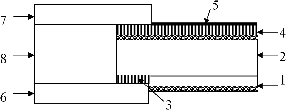
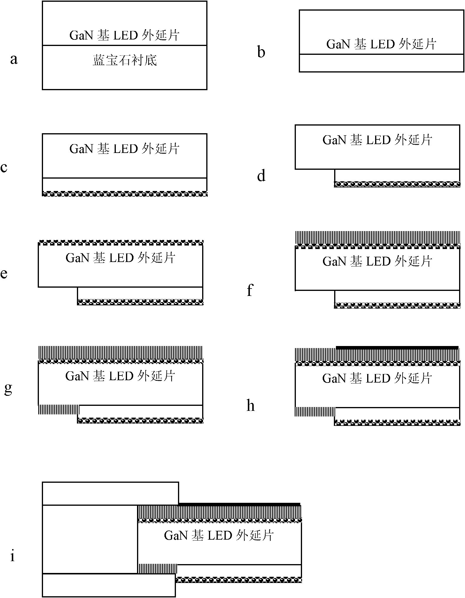
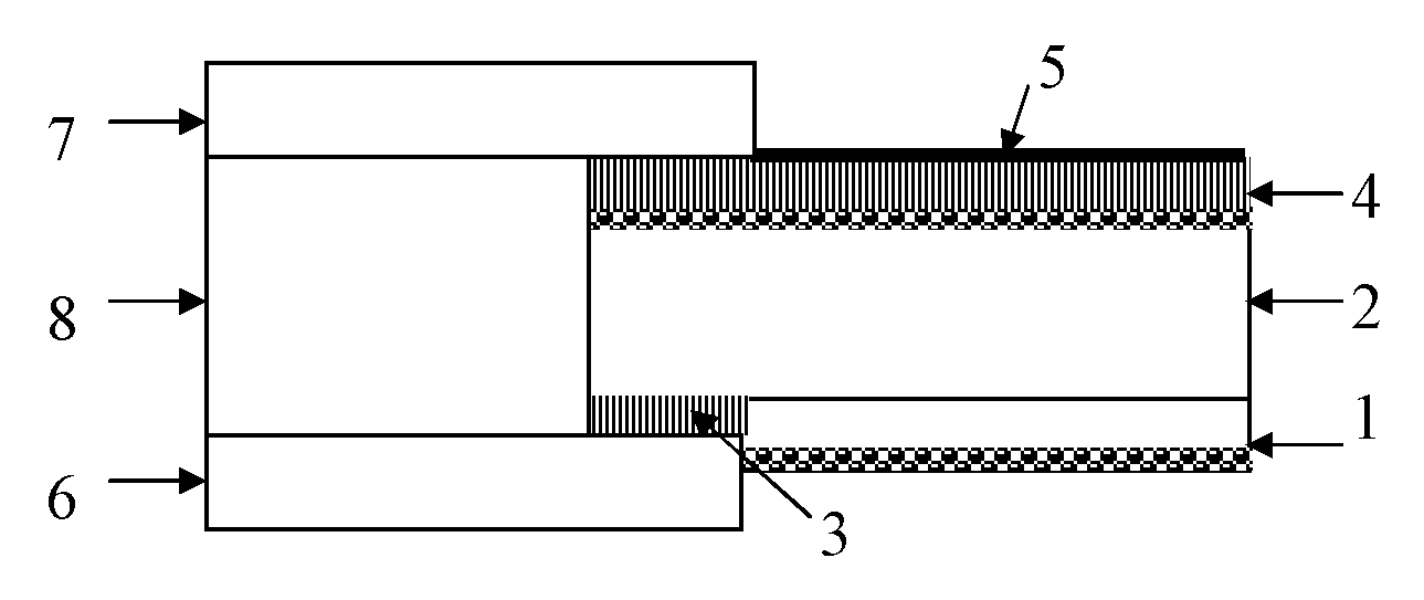
[0029] figure 1 It is a schematic diagram of the structure of the light emitting diode of the present invention. Such as figure 1 As shown, the light-emitting diode of the present invention includes a substrate 1 and an LED epitaxial wafer 2 grown on the substrate 1. The side of the LED epitaxial wafer close to the substrate 1 is an n-type layer, and the side of the LED epitaxial wafer far away from the substrate 1 is p-type layer. A first step is formed between the substrate 1 and the LED epitaxial wafer 2. An n-electrode 3 is provided at the first step. A first conductive and thermally conductive substrate 6 is provided outside the n electrode 3. The surface of the p-type layer of the LED epitaxial wafer 2 A p-electrode 4 and a protective layer...


PUM


Abstract

The invention discloses a light-emitting diode (LED) and a manufacturing method thereof. The LED comprises a substrate and an LED epitaxial wafer which grows on the substrate, wherein a first step is formed between the LED epitaxial wafer and the substrate, and is provided with an electrode n and a first current-conducting and heat-conducting substrate in sequence; the surface of the LED epitaxial wafer is provided with an electrode p and a protective layer in sequence; the electrode p and the protective layer form a second step; and the second step is provided with a second current-conducting and heat-conducting substrate. The manufacturing method comprises the following steps of: manufacturing the electrode n, the electrode p and the protective layer respectively based on the substrate on which the LED epitaxial wafer grows; and fixing the electrode n, the electrode p and the protective layer with current-conducting and heat-conducting substrates. The LED has the effect of conducting heat on double faces and emitting light on multiple faces, has the characteristics of high power, quick heat conducting speed, high light emitting efficiency, large light emitting angle and the like, and is free from glaring effect. The manufacturing method of the LED has a simple process flow and low cost, and is suitable for industrial production.

Description

Technical field [0001] The invention relates to the technical field of LED lighting, in particular to an LED and a manufacturing method thereof. Background technique [0002] Light-emitting diodes (LEDs) are a kind of light-emitting components, which are widely used in road lighting, automotive electronics and daily life lighting. [0003] The traditional LED has a planar electrode structure, that is, the p / n electrode and the light-emitting surface are on the same plane, and its preparation process and flow have been quite mature, and it has a dominant position in the low-power device market. However, the traditional LED structure has obvious limitations. Its heat dissipation, light extraction efficiency and chip utilization are relatively low, especially the heat dissipation effect is poor, and it cannot be used to manufacture high-power LEDs. [0004] In order to manufacture high-power LEDs, Lumileds and Cree respectively developed a flip-chip structure and a vertical structure, ...

Claims


Application Information

Patent Timeline
Patent Type & Authority Applications(China)
IPC IPC(8): H01L33/20
Inventor 周明杰刘舸
Owner OCEANS KING LIGHTING SCI&TECH CO LTD
Why Eureka
Try Eureka