Manufacturing method of connecting sheet circuit board

A technology for connecting a circuit board and a manufacturing method, which is applied in the directions of printed circuit manufacturing, printed circuits, electrical components, etc., can solve the problems of circuit board unit positioning shaking, large forming deviation, and non-compliance with forming accuracy requirements, so as to improve the forming process. Accuracy, the effect of ensuring molding accuracy

Inactive Publication Date: 2011-10-19
HONG HENG SHENG ELECTRICAL TECH HUAIAN +1
View PDF5 Cites 21 Cited by
  • Summary
  • Abstract
  • Description
  • Claims
  • Application Information

AI Technical Summary

Problems solved by technology

During the forming process, the copper-clad substrate is positioned on the machine through the positioning hole and cut to the last circuit board unit of each continuous circuit board, especially when the above-mentioned circuit board unit is far away from the connecting piece. , the circuit board unit will shake due to the weak positioning effect, and thus cause the forming deviation of the circuit board unit to be too large, which does not meet the requirements of forming accuracy and affect the overall performance of the circuit board
When the shape of each circuit board unit of the connected circuit board is long and narrow, for example, when the circuit board unit is an LED light strip circuit board, such large deviations in molding are more likely to occur

Method used


Image

  • Manufacturing method of connecting sheet circuit board
  • Manufacturing method of connecting sheet circuit board
  • Manufacturing method of connecting sheet circuit board

Examples


Embodiment Construction

[0040] The manufacturing method of the connected circuit board provided by the technical solution will be further described in detail below in conjunction with the accompanying drawings and embodiments.

[0041] The embodiment of the technical solution provides a method for manufacturing a continuous circuit board, which includes the following steps:

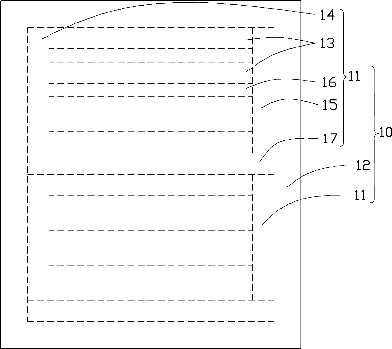
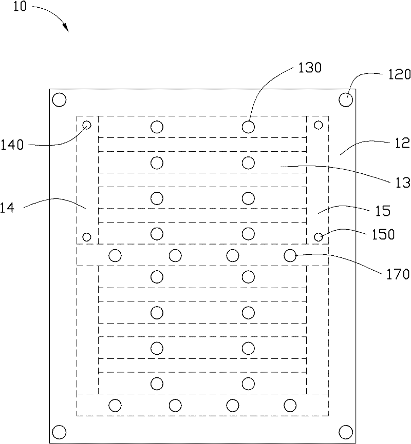
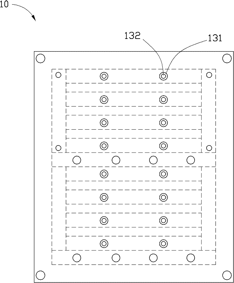
[0042] For the first step, please also refer to figure 1 and figure 2 , provide a copper-clad substrate 10, the copper-clad substrate 10 includes at least one processing area 11 and a first waste area 12 surrounding and connected to the at least one processing area 11. The copper-clad substrate 10 can be a rectangular double-sided copper-clad board, which includes a first conductive layer, an insulating layer and a second conductive layer stacked in sequence. In this embodiment, the processing area 11 is also rectangular, and its length direction is the width direction of the copper clad substrate 10 . The number of the proc...


PUM


Abstract

The invention relates to a manufacturing method of a connecting sheet circuit board, comprising the following steps: a copper cladding base plate is provided and comprises at least one processing area and a first waste area, wherein the at least one processing area comprises a plurality of product areas, a first connecting area, a second connecting area, at least one second waste area and an auxiliary locating area; a plurality of connecting locating holes are respectively arranged in the first connecting area and the second connecting area, a plurality of auxiliary locating holes are arranged in the auxiliary locating area, the copper cladding base plate is located on one worktable and is cut along the boundary of the at least one processing area, so as to remove the first waste area; and the copper cladding base plate is cut along the boundary of each second waste area sequentially from one second waste area furthest away from the auxiliary locating area, so as to remove a pluralityof the second waste areas; and the copper cladding base plate is cut along the boundaries of the auxiliary locating area and the product area connected with the auxiliary locating area, so as to remove the auxiliary locating area.

Description

technical field [0001] The invention relates to circuit board manufacturing technology, in particular to a method for manufacturing continuous circuit boards. Background technique [0002] The production of printed circuit boards generally includes the preparation of copper-clad substrates, the production of conductive lines on copper-clad substrates, and the placement, insertion or welding of circuit components. In order to facilitate downstream patching, plug-in or welding operations, it has gradually become a trend to make circuit boards into continuous circuit boards. A contiguous circuit board, also known as a disconnectable circuit board, includes a plurality of small-area circuit board units arranged side by side or arranged in an array. In the continuous circuit board, the adjacent circuit board units are cut during molding, and at the same time, a certain connection strength is retained through the connecting piece. In this way, after the process of patching, plug-...

Claims


Application Information

Patent Timeline
Patent Type & Authority Applications(China)
IPC IPC(8): H05K3/00
Inventor 卢国军张亮亮陈俊
Owner HONG HENG SHENG ELECTRICAL TECH HUAIAN
Why Eureka
Try Eureka