Solder joint stress reduction structure and printed circuit board comprising same

A printed circuit board and stress technology, applied in the direction of printed circuit components and electrical components to assemble printed circuits, can solve problems such as solder joint breakage, interruption, poor electrical connection between devices and printed circuit boards, etc., to reduce stress, The effect of preventing breakage

Inactive Publication Date: 2011-11-02
HUAWEI TECH CO LTD
View PDF5 Cites 10 Cited by
  • Summary
  • Abstract
  • Description
  • Claims
  • Application Information

AI Technical Summary

Problems solved by technology

If the solder joint is subjected to excessive stress, the solder joint may break, resulting in poor or interrupted electrical connection between the device and the printed circuit board

Method used


Image

  • Solder joint stress reduction structure and printed circuit board comprising same
  • Solder joint stress reduction structure and printed circuit board comprising same
  • Solder joint stress reduction structure and printed circuit board comprising same

Examples


Embodiment Construction

[0018] The following will illustrate the implementation of the present invention through specific examples, and those skilled in the art can understand other features and effects of the present invention through the content disclosed in the present invention.

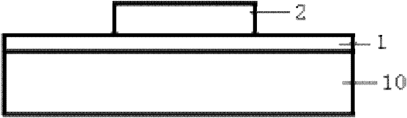
[0019] figure 1 is a schematic diagram showing a printed circuit board having a device mounted thereon according to the present invention, the printed circuit board including the solder joint stress relief structure according to the present invention. Such as figure 1 As shown, a device 2 is arranged on a printed circuit board 1 , and a supporting structure 10 such as a metal plate or a structural member is arranged under the printed circuit board 1 .

[0020] The device 2 is generally a package with a rectangular structure. For example, the device 2 can be a quad flat no-lead package (QFN), grid array package (LGA), chip-scale package (CSP), wafer-level package (WLP), A packaged device or module such as a ball grid a...


PUM


Abstract

The invention provides a solder joint stress reduction structure for reducing stress borne by a solder joint between a printed circuit board and a device welded on the printed circuit board. The solder joint stress reduction structure comprises an open slot. The open slot is formed on the printed circuit board and close to the device. The open slot can be positioned at a position close to an outer side of a corner of the device on the printed circuit board, or can be positioned at a position below the device on the printed circuit board. By arranging the solder joint stress reduction structure on the printed circuit board and close to the device, the stress borne by the solder joint between the device and the printed circuit board can be released or dispersed through the solder joint stress reduction structure, so that the stress borne by the solder joint is reduced; therefore, the phenomena that the solder joint is broken and the like are prevented. Moreover, the invention also provides the printed circuit board comprising the solder joint stress reduction structure.

Description

technical field [0001] The present invention relates to a solder joint stress relief structure, more particularly to a solder joint stress relief structure for reducing the stress suffered by solder joints in a printed circuit board and a printed circuit board comprising the structure. Background technique [0002] Printed circuit boards, also known as PCB boards or single boards, provide electrical and physical connections for various electronic components, devices or modules, so as to integrate these components, devices or modules together and realize the transmission of electrical signals. The printed circuit board uses an insulator plate as the base material, on which metal wires such as copper wires are used to provide wire connections for various components, devices or modules, thereby realizing the electrical connection between the various components. Various components, devices or modules are fixed on the printed circuit board by soldering. [0003] With the communi...

Claims


Application Information

Patent Timeline
Patent Type & Authority Applications(China)
IPC IPC(8): H05K3/34H05K1/02
Inventor 叶裕明李松林孙清杰严春美
Owner HUAWEI TECH CO LTD
Why Eureka
Try Eureka