

LED microarray packaging structure and manufacturing method thereof
A technology of packaging structure and manufacturing method, applied in semiconductor/solid-state device manufacturing, electrical components, electrical solid-state devices, etc., can solve the problems of cumbersome process, small level, and inability to achieve
- Summary
- Abstract
- Description
- Claims
- Application Information
AI Technical Summary
Problems solved by technology
Method used
Image

Examples
Embodiment Construction
[0033] The present invention will be further described in detail below in conjunction with the accompanying drawings and embodiments.
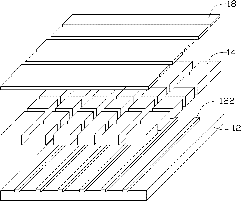
[0034] see figure 1 and Figure 11 One embodiment of the present invention provides an LED microarray packaging structure 100, which includes a substrate 12, a plurality of spaced first electrodes 122 disposed on the substrate 12, a plurality of LED chips 14 arranged in an array, and a plurality of second electrodes .
[0035] The substrate 12 is square in this embodiment, and its material can be copper or other suitable metals or metal alloys, such as aluminum or aluminum alloy, or other suitable non-metals, such as silicon and ceramics. The first electrodes 122 are disposed on the substrate 12 and insulated from the substrate 12 , and the first electrodes 122 are arranged at intervals corresponding to each row of the LED chip array 14 .
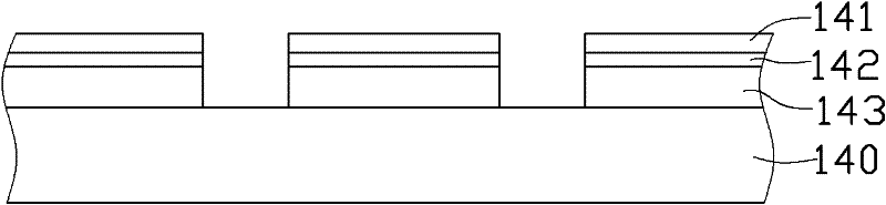
[0036] The LED chip 14 is a blue gallium nitride (GaN) LED chip in this embodiment. Of course, the L...
PUM
 Abstract
Description
Claims
Application Information