Suction cup and its holder

A wafer-bearing table and suction cup technology, which is used in electrical components, semiconductor/solid-state device manufacturing, circuits, etc., to achieve accurate and reliable positioning of wafers, accurate and reliable positioning, and more uniform adsorption effect.

Active Publication Date: 2011-12-07
SHANGHAI MICRO ELECTRONICS EQUIP (GRP) CO LTD +1
View PDF7 Cites 19 Cited by
  • Summary
  • Abstract
  • Description
  • Claims
  • Application Information

AI Technical Summary

Problems solved by technology

However, the existing patents or other documents do not involve the structure of the lower surface of the suction cup, and there is no clear description for optimizing the structure of the lower surface of the suction cup to position the wafer more accurately and reliably.

Method used


Image

  • Suction cup and its holder
  • Suction cup and its holder
  • Suction cup and its holder

Examples


Embodiment Construction

[0018] In order to better understand the technical content of the present invention, specific embodiments are given together with the attached drawings for description as follows.

[0019] Figure 1a It is a structural schematic diagram of the wafer stage module carrying wafers.

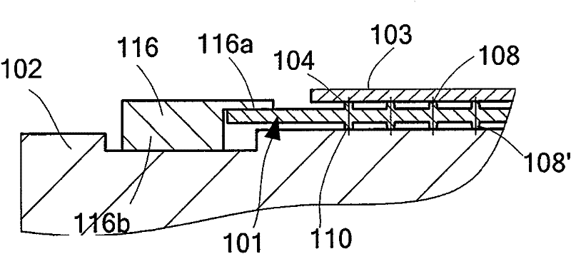
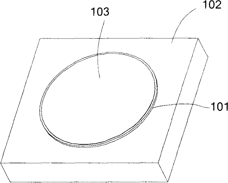
[0020] The wafer stage module mainly includes a suction cup 101 and a square mirror 102, where the wafer 103 is carried on the suction cup 101, and the suction cup 101 is circular and fixed on the square mirror 102 by vacuum, electrostatic adsorption or other methods. The upper surface of the square mirror 102 is mainly used to carry the suction cup 101 and the wafer 103 , and its lower surface is connected with a multi-degree-of-freedom actuator for adjusting its pose, thereby completing the positioning of the wafer 103 .

[0021] Figure 1b yes Figure 1a An exploded schematic diagram of the wafer stage module in .

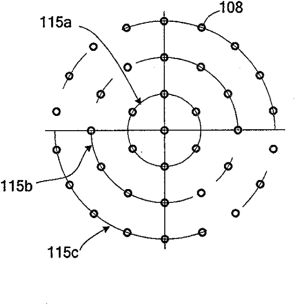
[0022] The present invention is based on the principle of vacuum adsorption. The...


PUM


Abstract

The invention provides a sucking disc and a chip supporting platform thereof. The lower surface of the sucking disk comprises a plurality of hollow annular bulges, a plurality of radial bulges and a plurality of vacuum through holes, wherein an annular cavity which does not pass through the upper surface and the lower surface of the sucking disk is formed in each hollow annular bulge; the annular cavity of at least one of the hollow annular bulges is provided with a vacuum communicating region; each radial bulge is arranged along the radial direction of the sucking disk and connects the hollow annular cavity with the vacuum communicating region to other hollow annular bulges; a radial hollow cavity which does not pass through the upper surface and the lower surface of the sucking disk is formed in each radial bulge, so that the radial bulges are communicated with the annular cavities in the hollow annular bulges; and the plurality of vacuum through holes are positioned in the annular cavities and pass through the upper surface and the lower surface of the sucking disk. Compared with the prior art, the sucking disk has the advantages that: due to adoption of the radial bulges with the radial hollow cavities, the vacuum connecting region can be quickly established in most part of the sucking disk quickly, so that the sucking effect of a sucking chip is more uniform and the chip can be positioned more precisely and reliably.

Description

technical field [0001] The present invention relates to a fixing device of lithography equipment, and in particular to a wafer carrying device used in lithography equipment, such as a wafer platform including a suction cup. Background technique [0002] The lithography equipment in the prior art is mainly used in the manufacture of integrated circuits (ICs) or other micro devices. Through photolithography equipment, multi-layer masks with different mask patterns are sequentially imaged under precise alignment on a wafer coated with photoresist, such as a semiconductor wafer or an LCD liquid crystal panel. [0003] A lithographic apparatus is an apparatus that images a mask pattern onto a wafer. Known lithographic apparatuses include step-and-repeat and step-and-scan. No matter what kind of lithography equipment, it is necessary to have a corresponding device as the carrier of the reticle and the wafer, and the carrier loaded with the reticle / wafer produces precise mutual m...

Claims


Application Information

Patent Timeline
Patent Type & Authority Applications(China)
IPC IPC(8): H01L21/683
Inventor 方洁齐芊枫李志龙
Owner SHANGHAI MICRO ELECTRONICS EQUIP (GRP) CO LTD
Why Eureka
Try Eureka