Single-side gate fin field effect transistor and manufacturing method thereof

A field-effect transistor and fin-shaped technology, applied in the field of single-side gate fin-shaped field-effect transistors

Inactive Publication Date: 2011-12-07
NAN YA TECH
View PDF2 Cites 9 Cited by
  • Summary
  • Abstract
  • Description
  • Claims
  • Application Information

AI Technical Summary

Problems solved by technology

[0005] The purpose of the present invention is to solve the problem of electrical coupling in DRAM due to the continuous reduction of word line spacing and the like.

Method used


Image

  • Single-side gate fin field effect transistor and manufacturing method thereof
  • Single-side gate fin field effect transistor and manufacturing method thereof
  • Single-side gate fin field effect transistor and manufacturing method thereof

Examples


Embodiment Construction

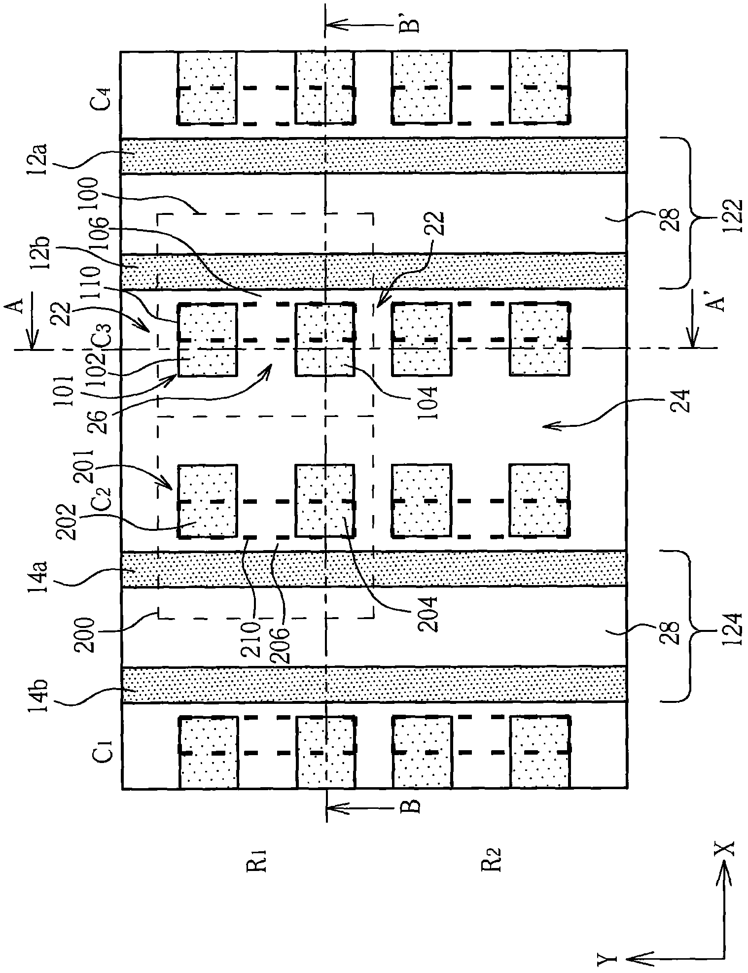
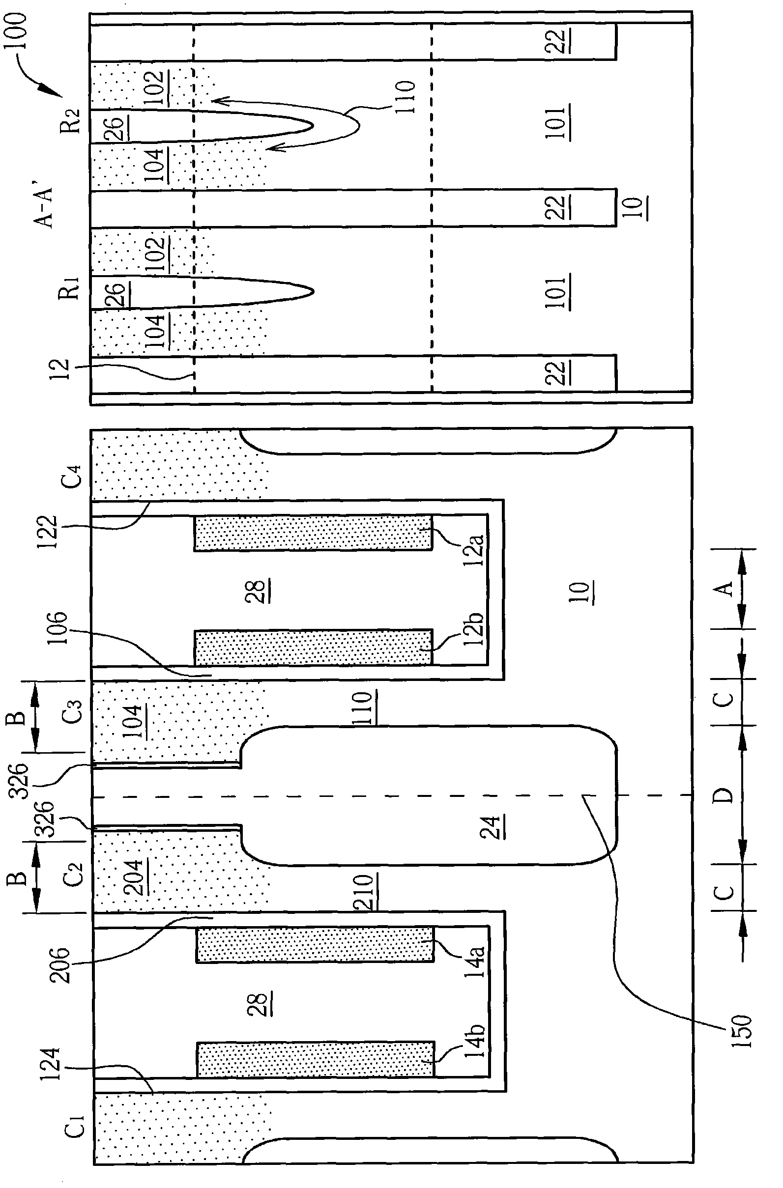
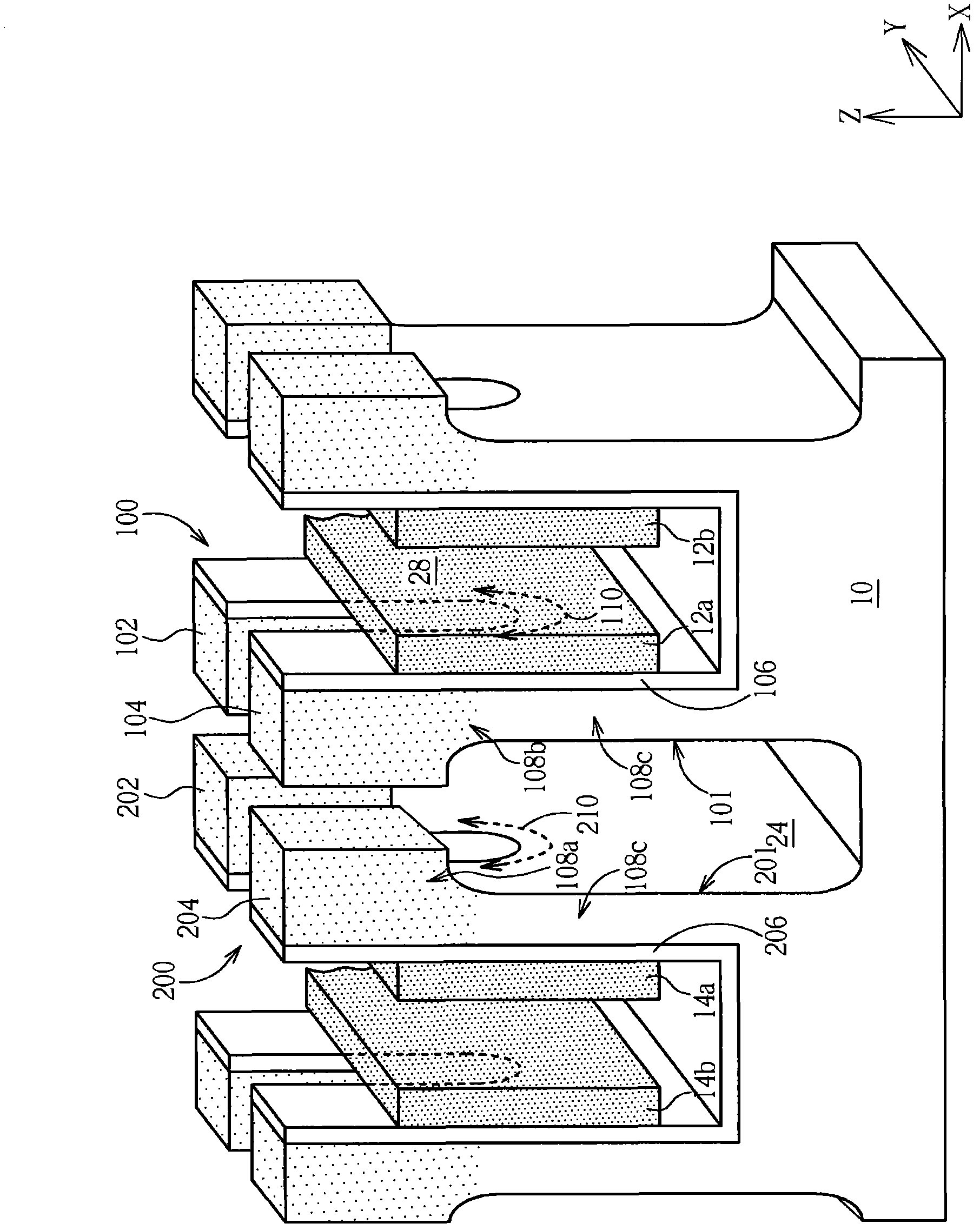
[0019] Although the present invention is disclosed as follows with examples, it is not intended to limit the present invention. Any person skilled in the art may make some changes and modifications without departing from the spirit and scope of the present invention. Therefore, the protection of the present invention The scope should be defined by the claims, and in order not to obscure the spirit of the present invention, details of some well-known structures and process steps will not be disclosed herein.

[0020] Likewise, the figures shown are schematic diagrams of the devices in the embodiments but are not intended to limit the size of the devices. In particular, in order to make the present invention more clearly presented, the sizes of some components may be enlarged in the figures. Furthermore, the same components disclosed in multiple embodiments will be marked with the same or similar symbols to make the description easier and clearer.

[0021] "Horizontal" referred ...


PUM


Abstract

A single-gate FinFET structure includes an active fin structure having two enlarged head portions and a tapered neck portion that connects the enlarged head portions with an underlying ultra-thin body. Two source / drain regions are doped in the two enlarged head portions respectively. An insulation region is interposed between the two source / drain regions. A trench isolation structure is disposed at one side of the tuning fork-shaped fin structure. A single-sided sidewall gate electrode is disposed on a vertical sidewall of the active fin structure opposite to the trench isolation structure.

Description

technical field [0001] The invention relates to a single-side gate fin-shaped field effect transistor, in particular to a single-side gate fin-shaped field-effect transistor with an ultra-thin base. Background technique [0002] DRAM is a type of random access memory that stores each bit of data in a capacitor on an integrated circuit. Generally speaking, the DRAM is arranged in a square array, and each memory cell is composed of a transistor and a capacitor. As a switching device, the transistor includes a gate and its next silicon channel channel region. The silicon channel region is located in the semiconductor substrate between a pair of source / drain regions, and the gate connects the source / drain regions electrically by controlling the silicon channel region. [0003] At present, the vertical double gate fin field effect transistor has been developed for the next 4F 2 DRAM technology generation, where F represents the minimum line width of the photolithography proces...

Claims


Application Information

Patent Timeline
Patent Type & Authority Applications(China)
IPC IPC(8): H01L29/78H01L27/108H01L21/336H01L21/8242
CPCH01L29/66818H01L27/10826H01L27/10879H01L29/7853H10B12/36H10B12/056
Inventor 任兴华
Owner NAN YA TECH
Why Eureka
Try Eureka