Manufacturing method of display panel and substrate for display device

A technology for display devices and display panels, applied in identification devices, lighting devices, semiconductor/solid-state device manufacturing, etc., to prevent water vapor and oxygen, prevent drive circuit degradation, and achieve long life effects

Inactive Publication Date: 2011-12-21
SUMITOMO CHEM CO LTD
View PDF8 Cites 2 Cited by
  • Summary
  • Abstract
  • Description
  • Claims
  • Application Information

AI Technical Summary

Problems solved by technology

On the other hand, in the case where the light-emitting layer is formed by a coating method, since it is necessary to separately apply a coating liquid to a predetermined area, the same problem as that of the vapor deposition method will arise.

Method used


Image

  • Manufacturing method of display panel and substrate for display device
  • Manufacturing method of display panel and substrate for display device
  • Manufacturing method of display panel and substrate for display device

Examples


Embodiment Construction

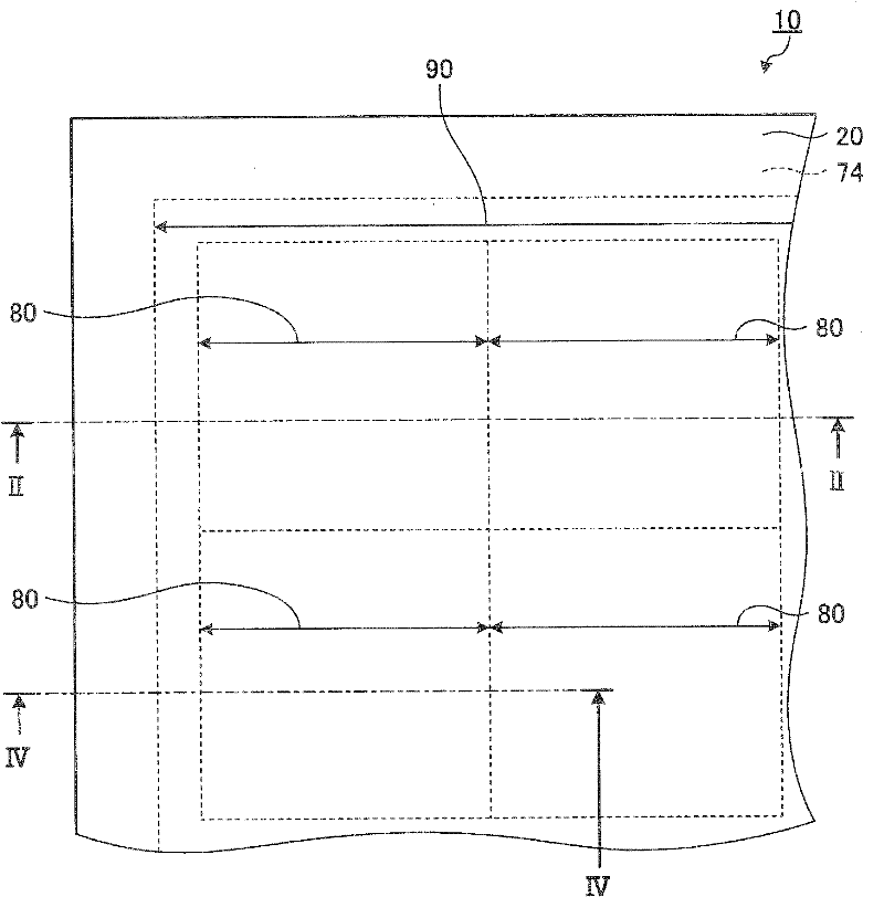
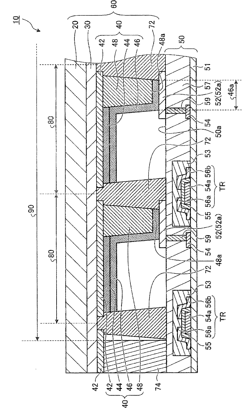
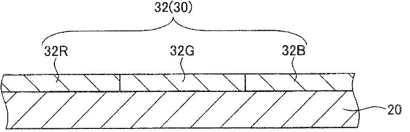
[0034] Hereinafter, embodiments of the present invention will be described with reference to the drawings. In addition, each figure schematically shows the shape, size, and arrangement|positioning of a component only for understanding of invention. The present invention is not limited to the following description, and each component can be appropriately changed within a range not departing from the gist of the present invention. In addition, in each figure used for the following description, the same code|symbol is attached|subjected to the same component, and the overlapping description may be abbreviate|omitted even in a different embodiment. In addition, although there are components such as electrode lead wires in the device on which the organic EL element is mounted, since they are not directly necessary in the description of the present invention, the description may be omitted. The device of the present invention equipped with an organic EL element does not necessarily...


PUM


Abstract

The present invention provides a method for manufacturing a display panel, comprising the following steps: a step of forming a substrate (60) for a display device, wherein a first substrate ( 20), a plurality of organic electroluminescent elements (40) each having the same configuration as the connection electrodes each having the connection terminal (46) formed thereon are arranged in a manner overlapping with the plurality of color filter elements, The process of forming a substrate (60) for a display device in this way; the process of preparing a substrate (50) for driving, which is equipped with a driving circuit for driving a plurality of organic electroluminescence elements, and is connected to the driving circuit. Connecting portion (52a) connected to it; the process of arranging a bonding member (74X) on the surface of the substrate for display device or the substrate for driving, so that in the state where the substrate for display device and the substrate for driving are bonded, the bonding member Surrounding a plurality of organic electroluminescence elements; the process of laminating the display device substrate and the driving substrate in such a way that the connection terminal and the connection part are in contact.

Description

technical field [0001] The present invention relates to a method of manufacturing a display panel including a plurality of organic electroluminescence (electroluminescence) elements (hereinafter also referred to as organic EL elements), a substrate for a display device used in the manufacturing method, and a display device comprising the same. A display panel using a substrate, and a display device including the display panel. Background technique [0002] Development of a flat-panel display (hereinafter sometimes referred to as "organic EL display device" or simply "display device") in which a self-luminous organic EL element is used as a light source for pixels is in progress. In an organic EL display device, a display panel that emits three colors of red, green, and blue light is installed, and the three colors of light are superimposed at a predetermined light intensity ratio, thereby enabling color display. [0003] In the case of a display panel for color display, thr...

Claims


Application Information

Patent Timeline
Patent Type & Authority Applications(China)
IPC IPC(8): H05B33/10G09F9/30H01L27/32H01L51/50H05B33/02H05B33/04H05B33/06H05B33/12
CPCH01L27/3253H01L27/322H10K59/38H10K59/1275H05B33/02H05B33/04H10K71/00
Inventor 西冈幸也栗原直梶谷优
Owner SUMITOMO CHEM CO LTD
Why Eureka
Try Eureka