Lens unit, aligning method, image pickup device and method for manufacturing image pickup device

A lens unit, camera device technology, applied in installation, electrical components, optical components, etc., can solve the problems of difficult optical axis alignment, difficulty, etc., and achieve the effect of good optical axis accuracy

Inactive Publication Date: 2012-01-04
KONICA MINOLTA OPTO
View PDF5 Cites 9 Cited by
  • Summary
  • Abstract
  • Description
  • Claims
  • Application Information

AI Technical Summary

Problems solved by technology

[0004] In addition, in such a compact imaging unit requiring high image resolution, the diaphragm tends to be placed on the most object side in consideration of telecentric performance (telecentricity). In this case, the lens unit is covered as an exterior part The opening of the lens frame case of the lens on the most object side is also used as the diaphragm mechanism, and there is also a structure covered by the diaphragm mechanism of other parts. There is a problem that it is difficult to align the optical axis, that is, it is difficult to see from the object side of the lens unit , observe the optical axis of the sensing unit to be sensed by light

Method used


Image

  • Lens unit, aligning method, image pickup device and method for manufacturing image pickup device
  • Lens unit, aligning method, image pickup device and method for manufacturing image pickup device
  • Lens unit, aligning method, image pickup device and method for manufacturing image pickup device

Examples


Embodiment 1

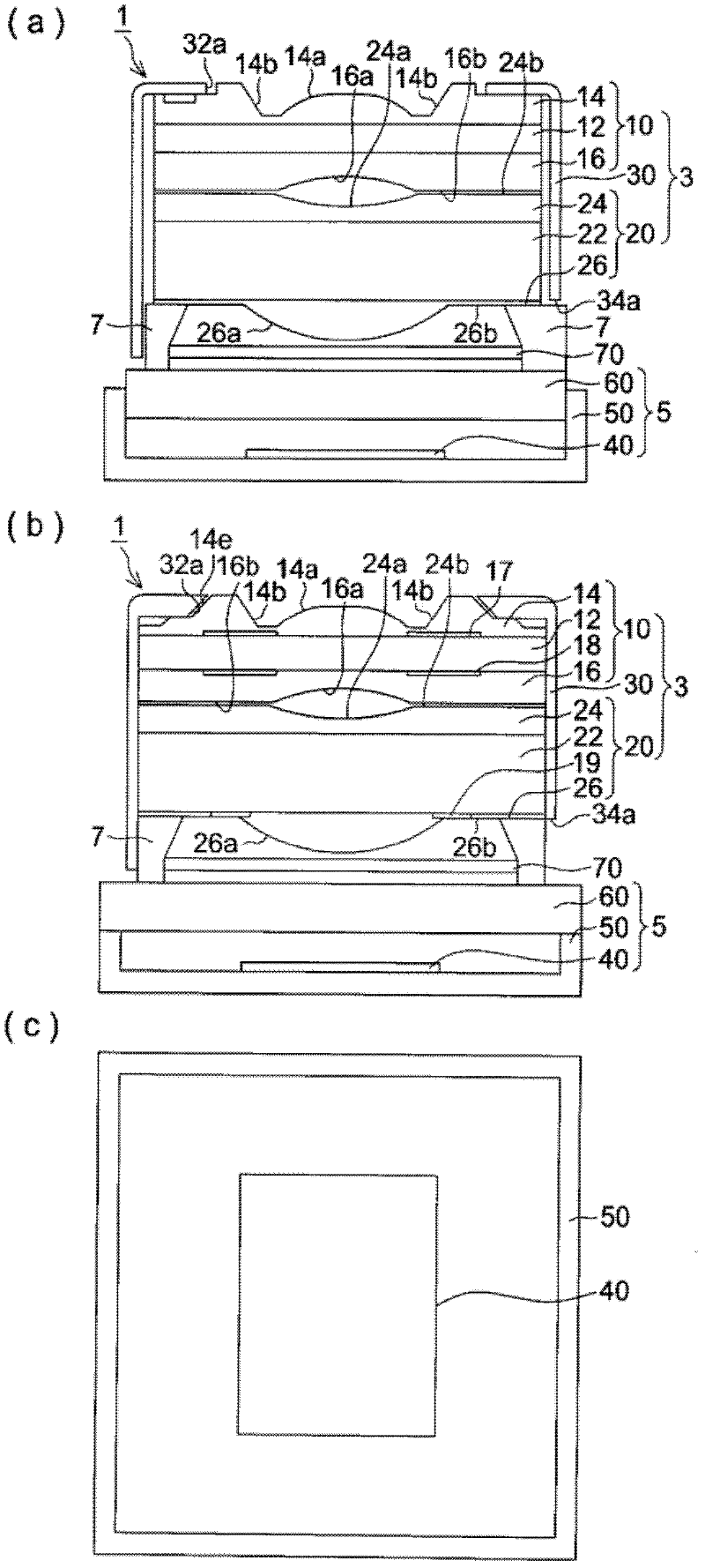
[0062] like figure 1 As shown in (a), the imaging device 1 of the preferred embodiment 1 of the present invention is mainly composed of a lens unit 3, a sensing unit 5, and a spacer 7, and the spacer 7 is interposed between the lens unit 3 and the sensing unit 5. structure.

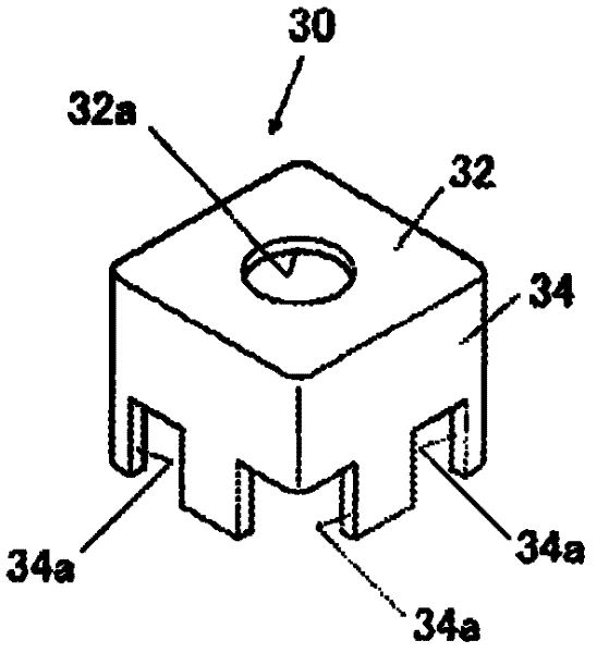
[0063] The lens unit 3 has wafer lenses 10 , 20 and a cover case 30 , and the wafer lenses 10 , 20 are covered by the cover case 30 in a state where the wafer lens 10 is laminated and bonded to the wafer lens 20 .

[0064] The wafer lens 10 has a flat glass substrate 12 . A molded portion 14 is formed on the upper surface of the glass substrate 12 , and a molded portion 16 is formed on the lower surface of the glass substrate 12 .

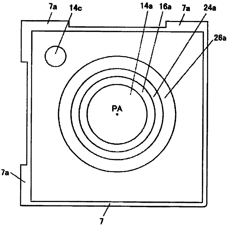
[0065] A convex lens portion (hereinafter also referred to as a convex lens portion) 14a is formed in the center of the molding portion 14, and an inclined portion 14b is formed on the molding portion 14 to incline upward from the convex lens portion 14a toward the outer per...

Embodiment 2

[0127] The main points different from Embodiment 1 in Embodiment 2 are as follows, and the others are the same as Embodiment 1.

[0128] like Figure 9 , Figure 10 As shown, in the imaging device 2 of the present embodiment 2, the inclined portion 14b and the spacer 7 (including the IR blocking filter 70) on the molding portion 14 of the wafer lens 10 are not provided, and as a structure replacing them, the molding of the wafer lens 20 A spacer portion 26c is formed on the portion 26 .

[0129] like Figure 9 , Figure 11 As shown, the spacer part 26c is composed of an inner inclined part 26d, a bonding part 26e, and an outer inclined part 26f, and is higher than the thickness of the convex lens part 26a.

[0130] The inner inclined portion 26d is inclined downward from the convex lens portion 26a toward the outer periphery. The bonding portion 26 e is flat and is a bonding surface to be bonded to the cover glass 60 of the sensor unit 5 . The outer inclined portion 26f ...


PUM


Abstract

Provided is a lens unit (3) wherein a plurality of wafer tenses (10, 20), each of which has resin molded sections (14, 16 (24, 26)) formed on a glass substrate (12 (22)) so as to have the optical axis of the wafer lens accord with that of a light receiving sensor, are laminated. In the molded section (14) of the wafer lens (10) arranged on the outermost side of the wafer lenses (10, 20), a sloped section (14b) for having an alignment jig abut thereon is formed.

Description

technical field [0001] The invention relates to a lens unit, a method for aligning the lens unit with a sensor, an imaging device using the alignment method, and a manufacturing method for the imaging device. Background technique [0002] In recent years, the manufacture of optical lenses is not a single molding. For example, there is a semiconductor manufacturing method that uses resin to simultaneously transfer and mold multiple micro-lens shapes on a glass substrate called a wafer to manufacture a wafer lens array and then singulate it. Techniques for forming so-called "wafer lenses" were developed. This technique is particularly useful for lenses for portable cameras, etc., which are required to be further miniaturized and mass-produced. [0003] In order to obtain higher image resolution, this kind of wafer lens is stacked and bonded with multiple wafer lens arrays, and then cut and singulated, and they are installed on the sensor, thereby enabling mass production of s...

Claims


Application Information

Patent Timeline
Patent Type & Authority Applications(China)
IPC IPC(8): G02B7/02H04N5/225H04N5/335
CPCH04N5/2257H04N5/2254G02B7/021Y10T29/49826H01L27/14618H04N23/57H04N23/55
Inventor 寺本东吾
Owner KONICA MINOLTA OPTO
Why Eureka
Try Eureka