TFT array substrate, and liquid crystal display panel
A technology of array substrate and substrate, applied in the field of liquid crystal display panel
- Summary
- Abstract
- Description
- Claims
- Application Information
AI Technical Summary
Problems solved by technology
Method used
Image

Examples
Embodiment approach 1
[0100] when based on figure 1 and figure 2 One embodiment of the present invention will be described as follows.
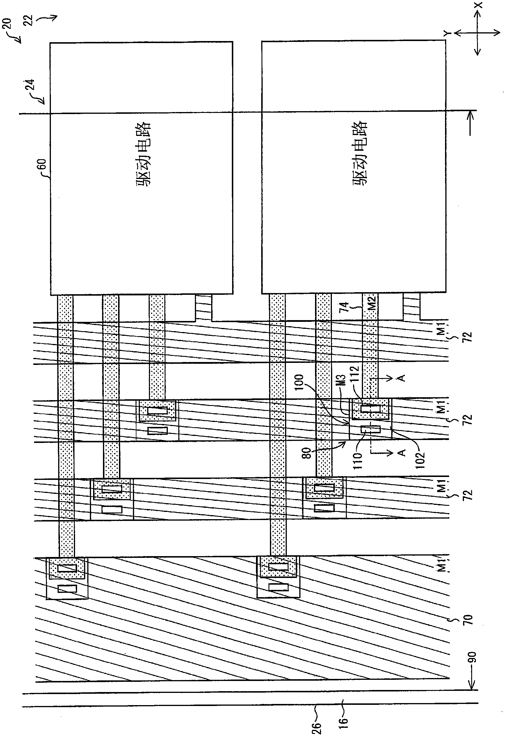
[0101] figure 1 It is a figure showing the schematic structure of the TFT array substrate 20 of this embodiment.
[0102] The TFT array substrate 20 of this embodiment has the same Figure 16 The described TFT array substrate 20 has almost the same schematic configuration.
[0103] That is, various wirings (wiring layers), driving circuits, and the like are provided in the peripheral region 24 of the TFT array substrate 20 .
[0104] Specifically, as various wirings, a low-potential-side power supply wiring 70 (signal wiring for scanning line driving circuit) as a trunk wiring and a clock wiring as a trunk wiring are provided along the Y direction of the TFT array substrate 20 . Line 72 (signal wiring for scanning line driving circuit). In detail, one low-potential side power line 70 is provided in the direction from the substrate edge 26 toward the displ...
Embodiment approach 2
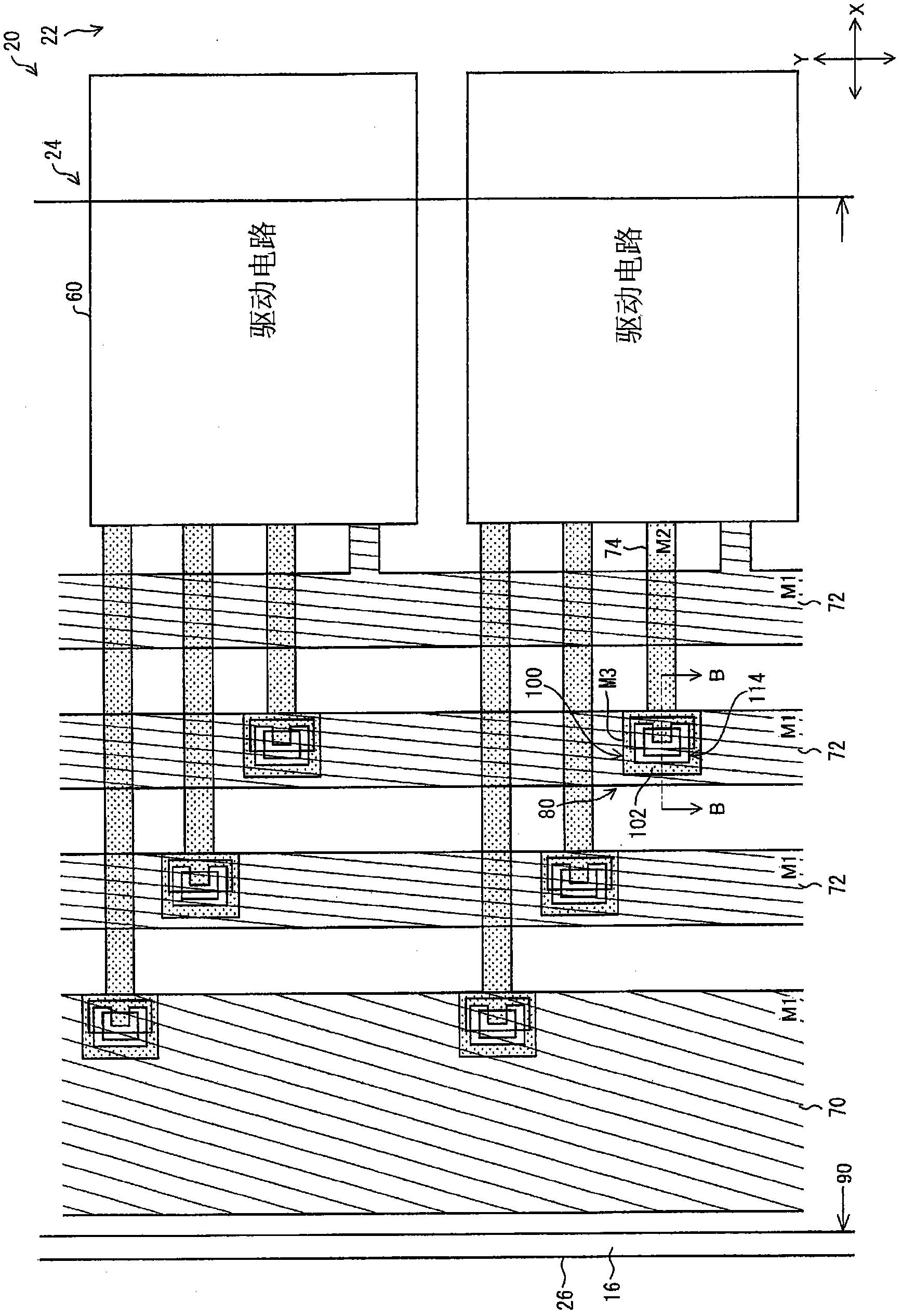
[0151] if based on image 3 and Figure 4 Other embodiments of the present invention will be described as follows. image 3 It is a figure showing the schematic structure of the TFT array substrate 20 of this embodiment. in addition, Figure 4 yes image 3 B-B line sectional view.
[0152] In addition, for convenience of description, components having the same functions as those in the drawings described in Embodiment 1 are denoted by the same reference numerals, and description thereof will be omitted.
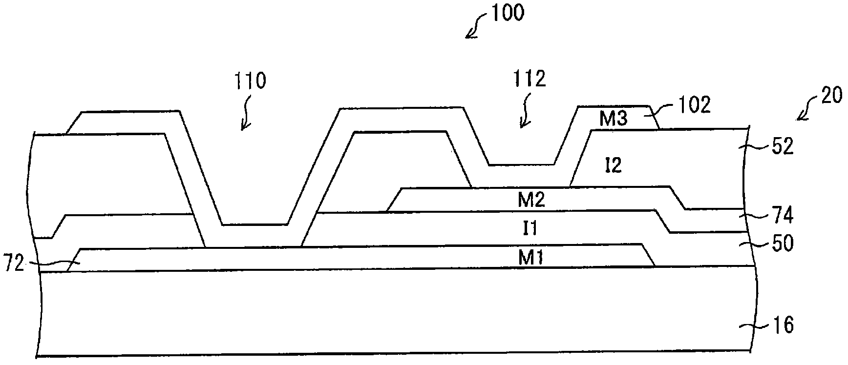
[0153] The TFT array substrate 2 of the present embodiment is different from the TFT array substrate 20 of the first embodiment in the form of the contact holes 100 .
[0154] Specifically, the contact hole 100 in this embodiment differs from the contact hole 100 in Embodiment 1 in the number of vias provided for one contact hole 100 .
[0155] That is, in the contact hole 100 of Embodiment 1, two paths of the main wiring path 110 and the branch wiring path 112 are prov...
Embodiment approach 3
[0173] if based on Figure 6 and Figure 7 Other embodiments of the present invention will be described as follows. Figure 6 and Figure 7 It is a figure showing the schematic structure of the TFT array substrate 20 of this embodiment.
[0174] In addition, for convenience of description, components having the same functions as those in the drawings described in the above-described embodiments are given the same reference numerals, and description thereof will be omitted.
[0175] The TFT array substrate 20 of this embodiment differs in the shape of wiring from the TFT array substrate 20 of the above-described embodiments. Specifically, the wiring extending in the Y direction is formed in a ladder shape.
[0176] exist Figure 6 and Figure 7 In the illustrated example, the low-potential-side power supply wiring 70 as the external wiring close to the substrate edge 26 is formed in a ladder shape.
[0177] Specifically, a rectangular notch 76 is provided on the low pote...
PUM
 Abstract
Description
Claims
Application Information
 - R&D
- Intellectual Property
- Life Sciences
- Materials
- Tech Scout
- Unparalleled Data Quality
- Higher Quality Content
- 60% Fewer Hallucinations
Browse by: Latest US Patents, China's latest patents, Technical Efficacy Thesaurus, Application Domain, Technology Topic, Popular Technical Reports.
© 2025 PatSnap. All rights reserved.Legal|Privacy policy|Modern Slavery Act Transparency Statement|Sitemap|About US| Contact US: help@patsnap.com