Method for obtaining space image of non-ideal lithography system based on Abbe vector imaging model
A technology of lithography system and imaging model, which is applied in the direction of microlithography exposure equipment, photolithography process exposure device, etc., can solve the problems of inapplicable resolution enhancement technology optimization method and no analytical expression given
- Summary
- Abstract
- Description
- Claims
- Application Information
AI Technical Summary
Problems solved by technology
Method used
Image

Examples
Embodiment
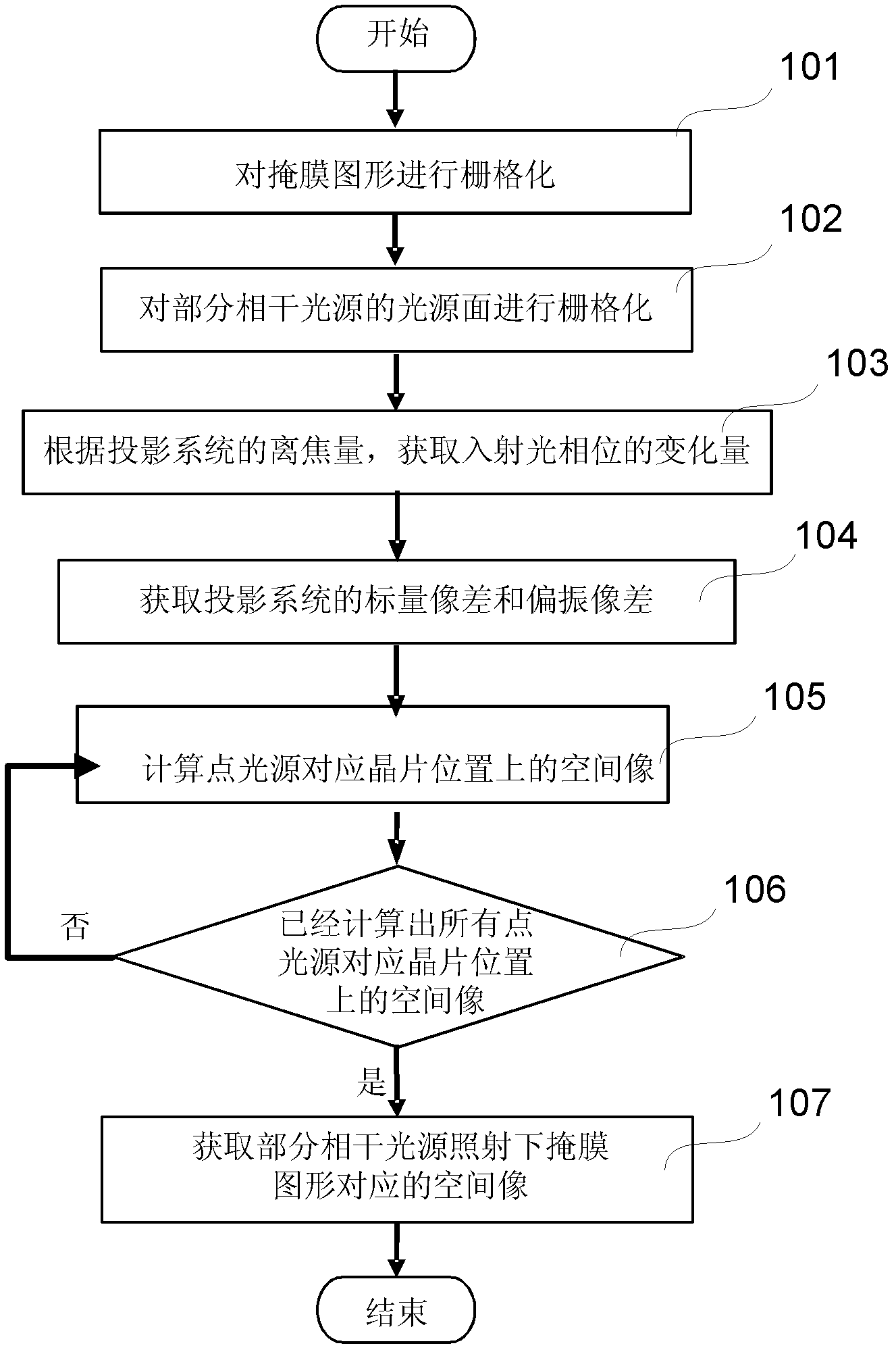
[0137] Such as Figure 5 As shown, the simulation uses the aberration obtained by ray tracing at a certain off-axis field of view point of the projection system designed in the laboratory (because in the field of numerical calculation, a two-dimensional figure is essentially a matrix. Here it is actually Draw the two-dimensional wave surface diagram corresponding to the scalar aberration matrix, and the value of each coordinate point on the diagram corresponds to the element value of the matrix one by one). 501 is a schematic diagram of the scalar aberration of the field of view point, and 502-509 are the eight Jones pupil components of the polarization aberration of the field of view point. 502 and 503 are respectively J xx The real and imaginary parts of . 504 and 505 are J respectively xy The real and imaginary parts of . 506 and 507 are J respectively yx The real and imaginary parts of . 508 and 509 are J respectively yy The real and imaginary parts of .
[0138] S...
PUM
 Abstract
Description
Claims
Application Information
 - R&D Engineer
- R&D Manager
- IP Professional
- Industry Leading Data Capabilities
- Powerful AI technology
- Patent DNA Extraction
Browse by: Latest US Patents, China's latest patents, Technical Efficacy Thesaurus, Application Domain, Technology Topic.
© 2024 PatSnap. All rights reserved.Legal|Privacy policy|Modern Slavery Act Transparency Statement|Sitemap